

HBM4 Brings Massive Memory Improvements
The flip side of the coin to all of that I/O bandwidth is MI455X’s memory bandwidth. For their new high-end accelerator, AMD needs to not only be able to quickly move data between the GPUs, but they need to be able to move data quickly within those GPUs. Much ink has been spilled over the subject of memory bandwidth for AI accelerators over the last several years now, and the basic requirements have not changed: AI accelerators need a massive amount of bandwidth in order to do training and inference at these large scales.
The solution to those needs now, as it has been ever since the Instinct line started almost a decade ago, has been High Bandwidth Memory. Pushing the limits of both DRAM manufacturing and chip packaging, HBM has become the industry’s bleeding-edge memory option by virtue of combining DRAM die stacking with very, very wide (and dense) memory buses between a host chip and its HBM stacks.
| HBM Memory Comparison | ||||||
| HBM4 | HBM3E | HBM3 | HBM2E | |||
| Max Capacity | 64 GB | 36 GB | 24 GB | 16 GB | ||
| Max Bandwidth Per Pin | 13.0 GT/s | 9.6 GT/s | 6.4 GT/s | 3.6 GT/s | ||
| Number of DRAM ICs per Stack | 16 | 12 | 12 | 8 | ||
| Effective Bus Width | 2048-bit | 1024-bit | ||||
| Bandwidth per Stack | 3.3 TB/s | 1.2 TB/s | 820 GB/s | 460 GB/s | ||
Now in its fourth major generation, HBM4 is, in many ways, the biggest change to the HBM technology standard since it was first introduced over a decade ago. Coming from HBM3(e), the critical change here is that the bus width of each HBM stack has been doubled: rather than 1024-bits wide, each stack now offers a 2048-bit wide memory bus. At iso-frequencies, this would double the amount of memory bandwidth available to a given HBM stack, which is a larger generational leap in memory bandwidth than we have seen over the past few iterations of HBM.
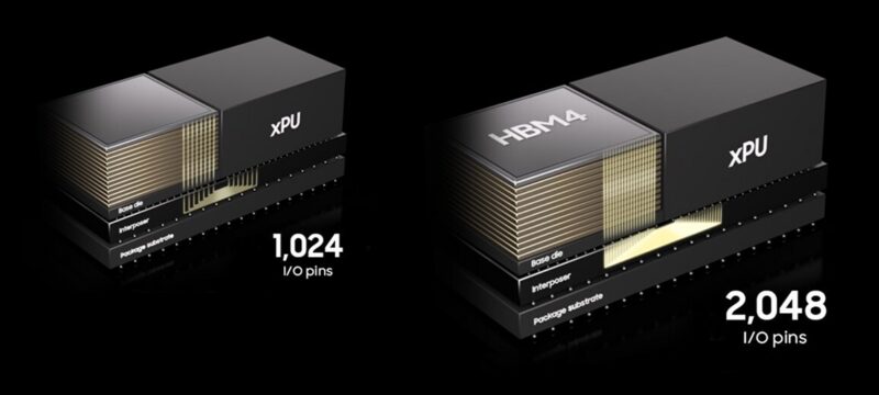
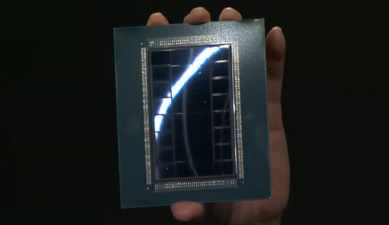
And AMD did not just settle for doubling the size of their memory bus. Rather than going with 8 stacks of HBM4 to replace the 8 stacks of HBM3e used in the MI350 series, AMD upped the ante to 12 stacks of HBM4, adding 4 more stacks to the total. As a result, the MI455X has a simply absurd memory bus that is effectively 24,576 bits wide, three times the bus width of the MI350 series.
It is this wider memory bus that is driving all of AMD’s DRAM bandwidth gains. In fact, MI455X’s memory bus is clocked slightly slower per pin than MI355X’s was, at roughly 7.6Gbps/pin versus 8Gbps/pin for the last-gen part. As a result, AMD has regressed in memory frequencies a bit going into the MI450 generation, but the vastly wider memory bus more than cancels out these losses. HBM was already a “wide” memory technology, but 12 stacks of HBM4 really takes that to a new level.
Now that we have the specifications for both the MI455X and NVIDIA’s rival Rubin GPU, it is also interesting to examine how the two companies are going in different directions in terms of bus sizes and memory frequencies. While NVIDIA is also using HBM4, the company has opted to use a narrower memory bus than AMD, sticking with 8 stacks of memory. But they are clocking it far higher, at around 10.7Gbps/pin. As a result, both Rubin and MI455X are quite close in memory bandwidth, with AMD holding a slight edge at 23.3TB/sec versus NVIDIA’s 22TB/sec.
This difference also plays into the memory capacity of both chips, and it is why AMD is going to be enjoying a more sizable advantage in memory capacity. With current HBM4 stacks maxing out at 36GB, 3GB dies arranged in a 12-Hi stack, AMD is able to install 50% more memory by virtue of having 50% more stacks. It is a simple calculation, but it is one that, for the first time, will give AMD a significant edge in total memory capacity for a single GPU.
The trade-off for AMD then is the complexity of routing that larger memory bus. Perfectly connecting 25K traces is no small matter. And for AMD’s chip engineers, they have to accomplish this while growing accustomed to using CoWoS-L for the very first time.
In any case, MI455X’s 432GB of HBM4 is evenly distributed between the two FCDs. Each die houses 6 HBM4 memory controllers and is attached to 6 of the HBM4 memory stacks. The Infinity Fabric connecting the two FCDs is fast enough that an MI455X can be configured to behave as a single chip inside a single NUMA domain, with addresses interleaved across all 12 memory stacks. Alternatively, the chip can be partitioned into two NUMA domains (NPS2 mode), where each FCD and its associated XCDs function as their own domain, avoiding having to send memory requests across to the other FCD and its attached memory stacks.
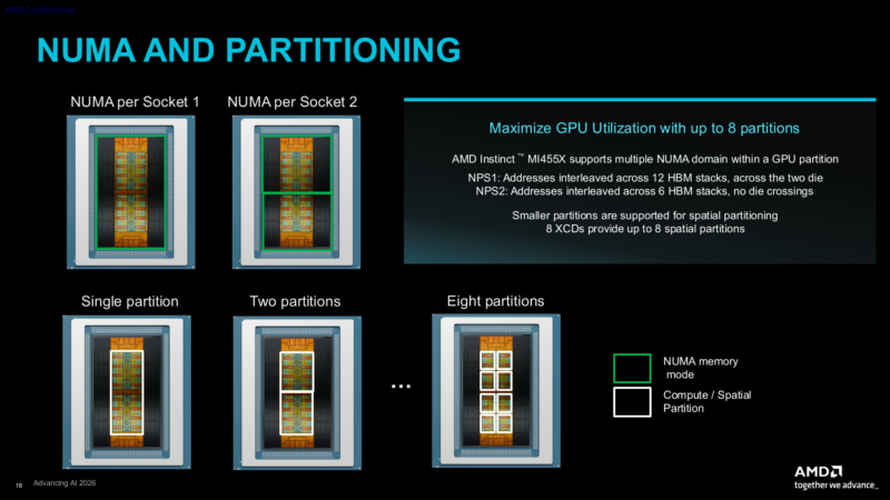
And though not a function of memory past this point, the MI455X can also be partitioned further. The chip can ultimately be partitioned to as small as a single XCD, allowing one MI455X to present itself as 8 devices. All of which are fully isolated from each other, of course.


The wide and slow (comparatively) HBM setup means AMD can take much lower bins of HBM, that would not meet the NVidia spec…cough Micron base die…
A smart move given the supply shortage, being able to scrape the barrel and take the dregs of HBM production.
Your write-up is spectacular, Ryan.
Thank you!
Thanks. I am glad you guys appreciate it.🙂
I’m on page two, and have two comments:
New process nodes do surprisingly little for increasing cache density, so while a lowering is surprising, not having a big increase wouldn’t be.
The usage of “chip” for the whole thing (as in “off chip links” is confusing. Each die is it’s own chip, after all. Saying “off package” would IMO be clearer.
@jaskij
So TSMC’s 2nm node is a GAAFET node. Unlike their 3nm node, it actually has a meaningful improvement on SRAM density. They are not massive gains like we used to get, but anything is better than nothing at this point.
Meanwhile, the usage of chip vs package is good feedback. Technically it is a chip comprised of multiple chiplets, but I do agree that package is less ambiguous.
great write up Ryan I really enjoyed it I’m just leaving a comment
I have lost hope to find again this level of writing around, but here it is and I’m so happy about it.
Thank you Ryan, and thanks to STH