

CDNA 5: AMD Gets Modern Under the Hood
The cornerstone to AMD’s server GPU efforts, the CDNA 5 architecture represents the biggest overhaul to AMD’s server GPU architectures since AMD split off server GPUs into CDNA almost a decade ago. For AMD, it is a necessary change on multiple levels, but it is also one that they have held back on for a surprisingly long period of time.
A Brief History of CDNA & GCN
Without getting too deep into the weeds of history here, the first four iterations of AMD’s CDNA architecture can all trace their origins back to AMD’s Vega architecture, which itself was the fifth and final mainstream iteration of AMD’s Graphics Core Next (GCN) architecture. First introduced by AMD in 2012 for consumer cards and then iterated upon and improved many times since then, the fundamental GCN architecture has been the backbone of AMD’s server GPUs for well over a decade at this point.
After branching from AMD’s mainstream chips in 2017 with the Vega (GCN5) architecture, each iteration of CDNA since then has added many new features to AMD’s GPU compute architecture. However, even with all of those changes, they were all fundamentally extensions of GCN and its 16-slot ALU structure. Internally, all of these resulting chips were part of what AMD calls their GFX9 architecture, which is the architecture classification for the Vega architecture and all of its derivatives.
But as time passes, all good things must come to an end. And so the end has come for GCN and the GFX9 architecture. AMD started to leave behind GCN in 2019 with the RDNA family of architectures for graphics chips, and now CDNA is doing the same for server accelerators, syncing up with RDNA to inherit many of its fundamental changes that have underpinned AMD’s graphics GPU architectures since then.
Waxing poetic over GPU architectures aside, let’s talk briefly about the fundamental changes going on here.
The single biggest change brought with CDNA 5 is that the underlying ALU/SIMD structure and execution model is widely different. Previously, AMD’s thread wavefronts were 64 threads wide, commonly referred to as Wave64. Each 64-thread wavefront would then occupy a 16-slot SIMD (SIMD16) for four cycles, with the SIMD processing a quarter of the wavefront in each cycle.
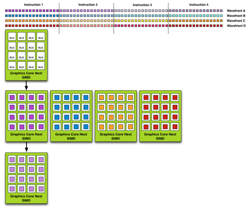
With 4 SIMD16s per CU, the resulting execution flow was designed to emphasize throughput, with (up to) 4 wavefronts being executed at a time, one quarter of a wavefront at a time. This gave GCN a 4-cycle latency to complete a Wave64 wavefront, which was an intentional design choice to help hide the latency of fetching the next instruction in a wavefront from memory.
The combination of Wave64 executing on top of a SIMD16 had its drawbacks, however: to fill a wavefront, the shader compiler (or human author) needed to be able to find 64 threads that could be grouped together, and there would always be that 4-cycle instruction latency. High concurrency is very efficient in terms of transistor usage (and is the same basic principle as tensor/matrix cores), but filling that kind of concurrency can be difficult.
Modern CDNA Gets Wider: Wave32 + SIMD32
Ultimately, AMD decided that the drawbacks to Wave64 + SIMD16 were too much in practice, and that they were not reaching the kind of high utilization/high performance that they wanted from GCN.
To remedy that, in 2019 for the first RDNA architecture (GFX10), AMD radically revised their GPU architecture. The size of wavefronts was cut down from 64 threads to 32 threads wide (Wave32), and the size of the internal SIMDs was expanded from 16 ALUs wide to 32 ALUs wide (SIMD32). Now, AMD’s GPU architecture could execute a single instruction from an entire wavefront in a single cycle. Among other benefits, this aligned AMD’s wavefront size with NVIDIA’s, reduced instruction latency, and improved SIMD utilization (and thus higher effective IPC rates) by allowing for smaller groupings of threads.
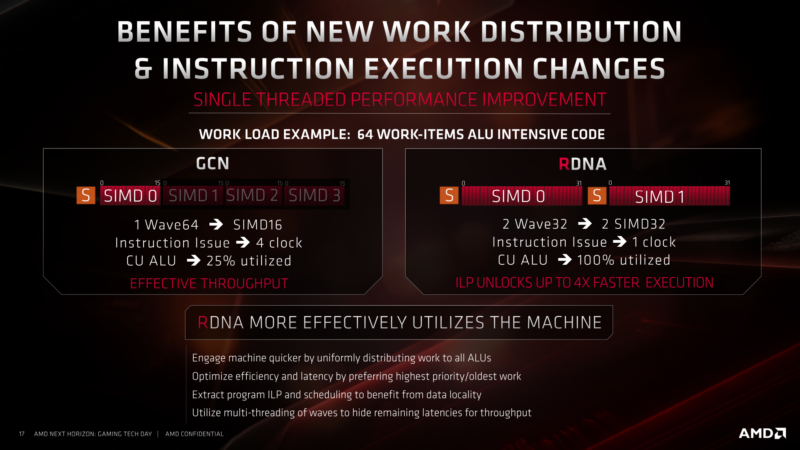
Bringing us back to the present, then, with the CDNA 5 architecture AMD is making a very similar shift. Gone are the SIMD16s and the native Wave64 wavefronts (though emulation is supported). In its place are SIMD32s and an emphasis on Wave32 wavefronts. It is nothing short of a generational GPU architecture change.
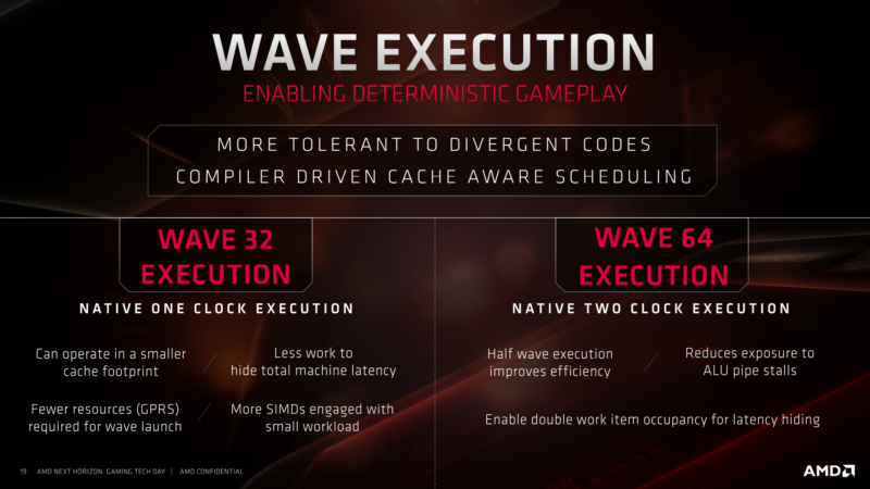
For AMD’s server GPUs, this will bring several changes. Perhaps the most fundamental one is simply the amount of work that can be done per cycle. AMD has replaced the SIMD16s wholesale with SIMD32s, meaning that for a given workgroup processor (WGP) configuration, CDNA 5 now has twice as much vector throughput as before. It is this change that is driving MI455X’s doubling of vector throughput, as the SIMDs executing all of those vector workloads are now twice as wide.
This also has the impact of cutting down on instruction latency, which was becoming a liability for AMD. Time-to-first-token and other latency measures are key metrics to AI performance, and requiring 4 cycles to resolve a single vector instruction (of which there are many in AI inference despite the emphasis on tensors) was not helping that.
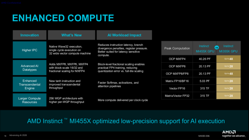
Meanwhile, the vector units were not the only enhancements in the CDNA 5 architecture. The matrix units, which like the vector units are packed 4 to a WGP, were given a throughput enhancement as well. At the baseline, each matrix unit can now process at least twice as many operations per clock with large tensors, effectively making each matrix unit twice as wide. Furthermore, for FP4 and FP8 in particular, AMD has improved performance there by even more, allowing CDNA 5 to process 4x as many operations per clock.
Consequently, while the high-level hardware figures do not necessarily indicate it, AMD has greatly enhanced the raw throughput (and really, the raw number of ALUs) within each one of their fundamental WGPs, and this is what is driving so much of MI455X’s peak compute throughput improvements. All of which sits in stark contrast to MI350, where a decent chunk of the peak performance improvements were driven by the addition of native support for smaller FP6/FP4 formats.
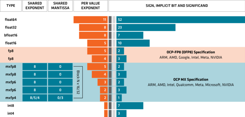
Speaking of number formats, while CDNA 5 does not bring anything new to the table for the matrix units in that regard, AMD has refined their matrix units by adding support for fractional scaling for the MXFP4 format. According to the company, this will allow for more efficient MXFP4 processing overall, and in particular it will help to reduce quantization errors when doing FP4 training.
The vector units, on the other hand, are getting support for one new numeric format, BFloat16 (BF16), which somehow escaped inclusion in AMD’s previous architectures.
Finally, AMD’s WGPs also feature new transcendental math units. The story here is much the same as the other blocks, with AMD doubling the throughput of the transcendental units. The updated units also gain support for a new instruction, hyperbolic tangents (tanh), which calculates the hyperbolic tangent of a number.
Working our way up AMD’s logical GPU architecture, despite the fundamental changes within each WGP, the larger compute architecture is relatively unchanged from CDNA 4. AMD has replaced the Compute Unit (CU) with the WGP as the fundamental compute core, but how they are organized is quite similar to before.
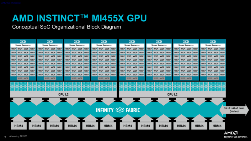
16 WGPs make up a single shader engine block. Two of these blocks (plus 2 spare WGPs for redundancy) are packed into a single XCD. Along with serving as the physical boundary for AMD’s compute hardware, the XCD level is where all shared frontend resources, such as the scheduler and asynchronous compute engines, are located.
With 8 XCDs, this gives MI455X a total of 256 WGPs. This is the same number of WGPs as on MI355X, but with the throughput improvements outlined earlier, it allows MI455X to process far more data even with the same number of WGPs.
CDNA 5 Cache and Memory Subsystem: A Bit Flatter and a Bit Wider
Along with the fundamental changes to AMD’s compute hierarchy in CDNA 5, the new GPU architecture also brings with it some important changes to AMD’s cache and memory hierarchy.
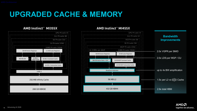
Visualized rather well by AMD’s slide, the big change here is that AMD has eliminated a whole layer of caching in its GPU architecture. Whereas CDNA 4 offered 3 layers of cache, L1, L2, and L3/Infinity Cache, the CDNA 5 architecture has removed the L2 cache as we know it. Instead of that small on-XCD cache, what was AMD’s Infinity Cache on the FCDs now serves as the chip’s L2 cache. Furthermore, that cache is smaller at 192MB for MI455X, versus 256MB for the MI355X’s Infinity Cache.
Internally, the L2 cache is split between the two FCDs, with each FCD containing 96MB of cache. This is further organized as 96 1MB SRAM blocks. According to AMD, there is an aggregate 54TB/second of bandwidth from the L2 cache (27TB/sec for each FCD), which, despite the shrink in capacity, is 3x the aggregate bandwidth of MI355X.
In another big change from CDNA 4, however, the access rules for the L2 cache have become more restrictive. Whereas CDNA 4 allowed WGPs to reach out to the Infinity Cache on either IOD, CDNA 5 restricts a WGP to only the L2 cache on its own FCD. There is no reaching out to the other FCD’s L2 cache. In effect, there are two 96MB L2 caches on the chip rather than one 256MB cache, as was the case on MI355X. We are told this was to improve how atomic operations are performed on the GPU architecture, and to reduce some of the overhead from keeping the FCDs’ caches in sync.
Moving on, on each XCD there is a new broadcast arbitrator for the memory hierarchy, which is there in part to make up for the lack of an XCD-level L2 cache. Among its functions, the arbitrator allows for memory reads to be multicast to multiple WGPs within a shader engine, rather than requiring each to make its own read, and ultimately conserving memory bandwidth usage. According to AMD, this is particularly useful for allowing the WGPs to fetch the weights and activations of an AI model all at once, as often they will all share the same values.
Finally, the local data store (LDS) cache size has also been buffed. Previously a 160KB cache exclusively for local data, it is now a 320KB cache that allocates 256KB for local data and another 64KB to vector caching. In effect, a larger L1 cache for CDNA 5; this helps to keep data closer to the WGPs and reduces the need to reach out to the L2 cache or beyond.
As with the L2 cache, the bandwidth to and from the LDS has also been improved. AMD does not list the specific figure, but says it is twice the bandwidth as on MI355X.
Moving beyond the memory hierarchy, AMD has also made a significant investment into improving general data movement in the CDNA 5 architecture, both to improve the efficiency of the architecture and to enable it to scale up to rack-scale levels suitable for Helios.
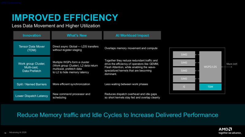
Among the highlights there, AMD has upgraded the tensor data mover (TDM) unit within each WGP, which works in conjunction with the matrix cores to asynchronously load data into them. In particular, AMD now allows it to move data between the LDS and DRAM, completely bypassing the WGP’s register file. We’re told that this is to reduce data movement overhead, latency, and free up compute units for other work.
And speaking of latency, AMD has also made further improvements throughout the architecture to reduce kernel launch latency. This is particularly helpful for small kernels, where a long launch time would greatly impact overall performance.
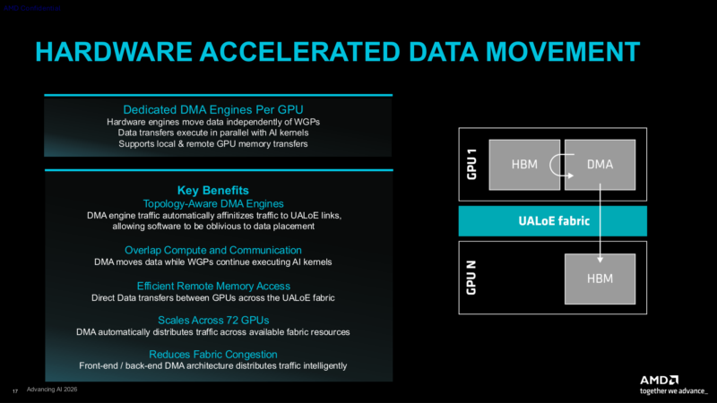
The larger DMA engines within the GPU architecture have also been given an overhaul, in part to better support scale-up networking. In effect, AMD has split its DMA engines into two pieces: the front-end, which remains visible in software, and a backend that is hidden from software. This abstraction allows the backend to handle data movement between nodes within a cluster without being explicitly commanded by the programmer in detail, offering a level of abstraction for DMA operations that allows programmers to avoid meticulously managing data across a full rack-scale system. Consequently, software running on MI455X clusters has the physical addresses of the system obscured as well so that an entire rackscale cluster appears and behaves as a single system.
This also helps AMD to keep data movement balanced across the many UALoE links within a rackscale system, as the hardware can split a DMA request and execute it over the most efficient number of links within a scale-up domain.


The wide and slow (comparatively) HBM setup means AMD can take much lower bins of HBM, that would not meet the NVidia spec…cough Micron base die…
A smart move given the supply shortage, being able to scrape the barrel and take the dregs of HBM production.
Your write-up is spectacular, Ryan.
Thank you!
Thanks. I am glad you guys appreciate it.🙂
I’m on page two, and have two comments:
New process nodes do surprisingly little for increasing cache density, so while a lowering is surprising, not having a big increase wouldn’t be.
The usage of “chip” for the whole thing (as in “off chip links” is confusing. Each die is it’s own chip, after all. Saying “off package” would IMO be clearer.
@jaskij
So TSMC’s 2nm node is a GAAFET node. Unlike their 3nm node, it actually has a meaningful improvement on SRAM density. They are not massive gains like we used to get, but anything is better than nothing at this point.
Meanwhile, the usage of chip vs package is good feedback. Technically it is a chip comprised of multiple chiplets, but I do agree that package is less ambiguous.
great write up Ryan I really enjoyed it I’m just leaving a comment
I have lost hope to find again this level of writing around, but here it is and I’m so happy about it.
Thank you Ryan, and thanks to STH