

Chiplets Still Rule, While Packaging Advances with CoWoS-L
Kicking off our deep dive into MI455X, we will take things literally and work our way down into the chip’s architecture. This means our first stop is at the chiplet level.
For MI455X, AMD has retained its strategy of stacking compute chiplets (XCDs) on top of the base die, which was first introduced with the MI300. Just like the MI350 series, we are looking at 8 compute dies placed over a pair of larger dies, which AMD is now more descriptively calling the Fabric and Cache Dies (FCDs). Finally, abutting (but not placed on top of) the FCDs are the new I/O dies (IODs), which now better live up to the name by being dedicated to chip I/O.
Notably, compared to NVIDIA, this stacked approach remains a unique design point for AMD’s server GPUs. Even NVIDIA’s forthcoming Rubin GPU will not employ this technique.

For AMD, the rationale behind this strategy has not changed: chiplets let AMD defray risks by producing multiple smaller dies rather than one or two dies that would naturally yield lower, and it allows AMD to mix and match process nodes to balance performance needs with cost and wafer availability. In practice, this means that AMD is shifting the risk from chip yields to advanced packaging yields, betting that the losses from bad die-to-die bonds will be lower than the losses from bad dies.
As noted earlier, the compute chiplets on MI455X are produced on TSMC’s N2 (2nm) process node, which is the company’s bleeding-edge process node. Along with fellow juggernaut Apple, AMD is one of the lead customers for the process node, with the company investing its precious N2 wafer allocations into building new server hardware. To make the NVIDIA comparison again, this means that AMD will once more have a process node advantage over NVIDIA, as AMD will be using N2 while NVIDIA uses N3P, mirroring the last generation where AMD was on N3 when NVIDIA was on N4.
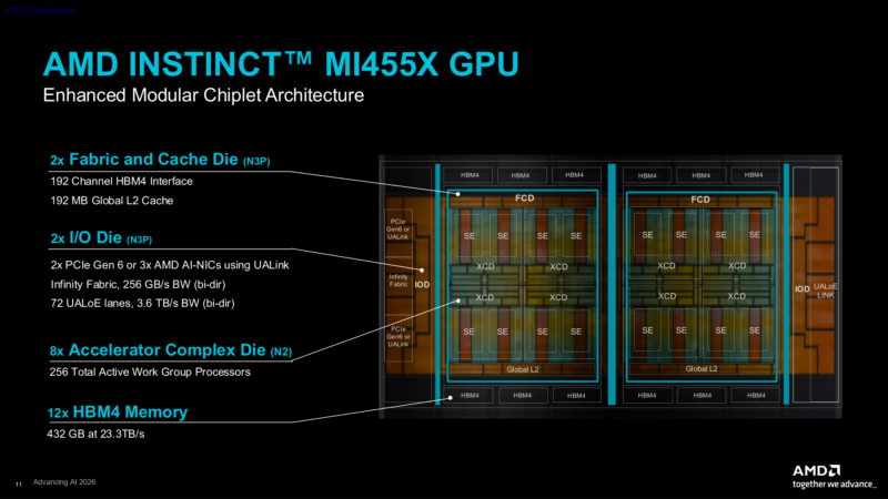
The organization within each XCD has changed since the CDNA 4 generation (more on that in a second) but the general purpose has not. These remain the location of AMD’s performance-critical compute blocks.
Meanwhile, the FCDs are once again being made on a trailing node, with AMD tapping TSMC’s N3P process node for these dies. While less performance-sensitive than the XCDs, the FCDs still have an important role in AMD’s GPU designs as they are where the extensive Infinity Fabric network is located, which is the portion of the chip that interconnects all of the different functional blocks of the GPU. It is also where the chip’s L2 cache is located (and hence Fabric and Cache Die), as well as AMD’s HBM memory controllers. For these reasons, the FCD has undergone a major grow-up of its own. Whereas the MI350 generation used TSMC’s tried-and-true N6 process node, for MI455X AMD has skipped right past all of TSMC’s 5nm-class nodes to land on N3P.
As with the MI350 series, there are two FCDs per GPU. Each one seats 4 XCDs, and it has extensive connectivity to both the other FCD as well as the new IODs. In some ways, the new FCDs are simpler than the IODs they replace because AMD has excised the off-chip I/O almost entirely. That leaves just the fabric, the cache, and the memory controllers as the major elements of the FCD.
Speaking of cache, surprisingly, AMD has actually cut down on the amount of cache on the FCDs. We will get into this a bit more when talking about the CDNA 5 architecture, but whereas the MI350 series IODs had a total of 256MB of cache, the MI455X FCDs only have 192MB of cache. This is despite the fact that AMD skipped multiple process nodes. So although AMD is not disclosing the die size or transistor counts of the individual dies on MI455X, the FCDs have likely not grown by as much as we would otherwise expect.
Finally, adjacent to each FCD are the new IODs, which, true to their name, handle off-chip I/O for the GPU. Specifically, the IODs hold the SerDes and related circuitry for the UAL/UALoE links, the xGMI link to the CPU, and the PCIe Gen6 links. The IODs are identical, but their role varies depending on which end of the MI455X they are on. On the far edge of the chip (facing the back side of a server tray), the IOD is dedicated entirely to UALoE links for the scale-up network. Meanwhile, on the near edge of the chip (facing the CPU and front side of a server tray) are the xGMI links and flexible links that can be used for either PCIe or UAL.
Like the FCDs, the IODs are made on a trailing-edge process node with TSMC’s N3P.
Stitching all of this together, in turn, is a new version of TSMC’s advanced packaging technologies: CoWoS-L. Ever since AMD first began using HBM-type memories, AMD has been relying on TSMC’s classic chip-on-wafer-on-substrate (CoWoS-S) packaging technology. Which, true to its name, CoWoS-S worked by placing a chip on top of a silicon interposer (the wafer part of CoWoS). This was a very effective strategy since silicon interposers were simplified chips that could be built with far smaller and denser connections than organic packaging could support. However, the trade-off was that the interposer needed to be large enough to have all of the dies in a chip design placed on top of it, and that ran into photolithography reticle limits.
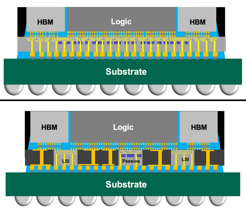
To that end, chip packaging firms (including TSMC) have developed newer variants of CoWoS that rely on using just small slices of silicon, local silicon interconnects (LSIs), rather than a massive chip-sized interposer. This maintains the connection density benefits of using silicon as the interconnection medium, but without the major drawbacks of the large interposer. (The best-known example of this chip packaging technique is Intel’s EMIB, though they are not the only company to use it these days)
For AMD, in turn, the switch to CoWoS-L allows them to more easily scale up their chip designs. The company has not disclosed the pitch of the CoWoS connections, so we cannot do a numeric comparison with CoWoS-S used on MI350, but the gist is that this is a more flexible option for AMD. And it is a pretty big change after using CoWoS-S for the last 12 years.


The wide and slow (comparatively) HBM setup means AMD can take much lower bins of HBM, that would not meet the NVidia spec…cough Micron base die…
A smart move given the supply shortage, being able to scrape the barrel and take the dregs of HBM production.
Your write-up is spectacular, Ryan.
Thank you!
Thanks. I am glad you guys appreciate it.🙂
I’m on page two, and have two comments:
New process nodes do surprisingly little for increasing cache density, so while a lowering is surprising, not having a big increase wouldn’t be.
The usage of “chip” for the whole thing (as in “off chip links” is confusing. Each die is it’s own chip, after all. Saying “off package” would IMO be clearer.
@jaskij
So TSMC’s 2nm node is a GAAFET node. Unlike their 3nm node, it actually has a meaningful improvement on SRAM density. They are not massive gains like we used to get, but anything is better than nothing at this point.
Meanwhile, the usage of chip vs package is good feedback. Technically it is a chip comprised of multiple chiplets, but I do agree that package is less ambiguous.
great write up Ryan I really enjoyed it I’m just leaving a comment
I have lost hope to find again this level of writing around, but here it is and I’m so happy about it.
Thank you Ryan, and thanks to STH