

Final Words
Wrapping things up on this GPU deep dive, AMD has given us a great deal to think about with the CDNA 5 architecture and the first server GPU built around it: Instinct MI455X. CDNA 5 marks AMD’s most ambitious server GPU to date, and in the process, AMD has left almost no aspect of the architecture untouched in one way or another.
Though few people will ever interact with these GPUs on a core SIMD level, the switch from Wave64 + SIMD16 to Wave32 + SIMD32 has been a long time coming. It marks the final passing of the torch from the GCN architecture that has defined over a decade of AMD GPUs, and which has been the cornerstone of the Instinct lineup since it began. The use of wider SIMDs and narrower wavefronts sets the stage to pay some significant dividends to AMD when it comes to instruction latency as well as hardware throughput, all of which reverberates through the rest of the architecture.
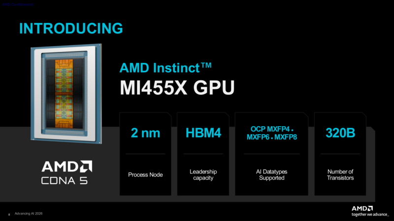
Speaking of throughput, no small amount of the performance improvement brought by CDNA 5 and the MI455X comes due to the amount of hardware AMD is throwing at the chip. Thanks to TSMC’s N2 process node, AMD has been able to double the width of its vector units, double the width of its matrix cores, and further optimizations have improved its performance even more for the all-important low-precision FP8 and FP4. If only by this virtue alone, MI455X stands to be a major step up from the current-generation MI355X.
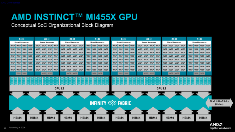
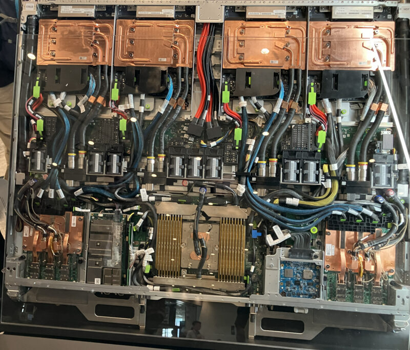
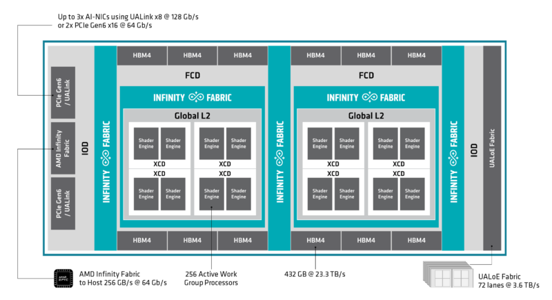
But the bigger story can be found in the bigger picture – and AMD’s need to evolve the CDNA 5 architecture to allow for rack-scale computing. The I/O bandwidth improvements of MI455X dwarf the raw performance improvements. The chip has nearly four times the I/O bandwidth, built on the back of a complex network of UALink-over-Ethernet transceivers. It is these critical network enhancements that allow MI455X to scale up to as many as 72 GPUs in a single domain, leaving the 8-way MI355X series in the dust. The need to support this kind of I/O bandwidth has touched virtually every aspect of the chip’s design, from how it is packaged to how the internal Infinity Fabric network operates.
Meanwhile, we would be remiss not to mention AMD’s heavy investment into memory bandwidth and memory capacity here. While the MI350 accelerators were already at the cutting-edge for their time with 8 stacks of HBM3e memory, AMD’s decision to go with 12 stacks of HBM4 memory is a big one, both figuratively and literally. The number of traces needed to wire up the ridiculous 24,576-bit memory bus is an achievement in and of itself, never mind the performance impact that a 23.3 TB/second of memory bandwidth brings to the table.
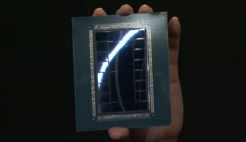
The end result is that MI455X and its underlying CDNA 5 architecture are pushing the envelope for AMD’s server GPUs in virtually every aspect possible. AMD has seemingly left no stone unturned here as they seek to continue their recent success in the server GPU market, laying the groundwork for not just faster GPUs, but for the next era of Instinct accelerators altogether.
Between MI455X, EPYC Venice, and of course, Helios, AMD has lofty ambitions for the world of server hardware and AI systems. It will be very interesting to see how all of this pans out over the next year as the first systems start shipping in the fourth quarter of this year.


The wide and slow (comparatively) HBM setup means AMD can take much lower bins of HBM, that would not meet the NVidia spec…cough Micron base die…
A smart move given the supply shortage, being able to scrape the barrel and take the dregs of HBM production.
Your write-up is spectacular, Ryan.
Thank you!
Thanks. I am glad you guys appreciate it.🙂
I’m on page two, and have two comments:
New process nodes do surprisingly little for increasing cache density, so while a lowering is surprising, not having a big increase wouldn’t be.
The usage of “chip” for the whole thing (as in “off chip links” is confusing. Each die is it’s own chip, after all. Saying “off package” would IMO be clearer.
@jaskij
So TSMC’s 2nm node is a GAAFET node. Unlike their 3nm node, it actually has a meaningful improvement on SRAM density. They are not massive gains like we used to get, but anything is better than nothing at this point.
Meanwhile, the usage of chip vs package is good feedback. Technically it is a chip comprised of multiple chiplets, but I do agree that package is less ambiguous.
great write up Ryan I really enjoyed it I’m just leaving a comment
I have lost hope to find again this level of writing around, but here it is and I’m so happy about it.
Thank you Ryan, and thanks to STH