
The Xilinx T1 is a new FPGA solution for the Open Radio Access Network or ORAN market. With the new card, Xilinx hopes to provide customers with an open solution to build virtualized infrastructure, from commodity components, for 5G markets. It also is a furthering of a theme from Xilinx that the company is selling cards with integrated IP.
Xilinx T1 Overview
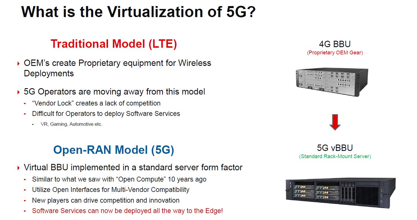
Taking a step back, you may have seen this 5G content and even reviews such as the recent Inspur NE5260M5 server review we just did on STH. Xilinx has a great slide about why. Effectively in the 4G LTE market, service providers used different proprietary OEM gear. As the operators want to deliver services at the edge, the idea of having virtualized infrastructure made of more commoditized hardware, that can be programmed in an agile manner has become more popular.
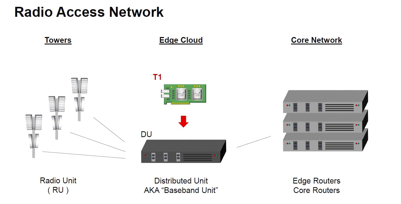
To make this kind of ORAN 5G network work, one needs to take radio signals, convert them into data that can be fed to and from the service providers’ network. The Xilinx T1 fits in what is called the baseband unit or distributed unit.
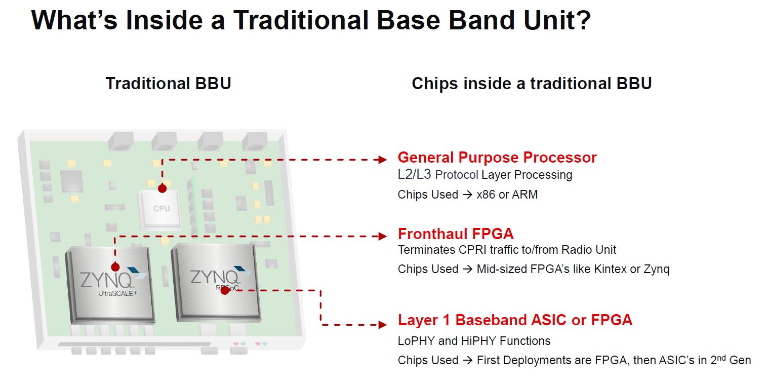
Inside the traditional baseband unit, there is either an x86 (Intel) or Arm (soon NVIDIA?) CPU such as the new Marvell OCTEON family. That is the L2/L3 chip but there are often two more chips. One is usually a fronthaul FPGA, which is Xilinx’s specialty, and othe other is a baseband ASIC or FPGA.
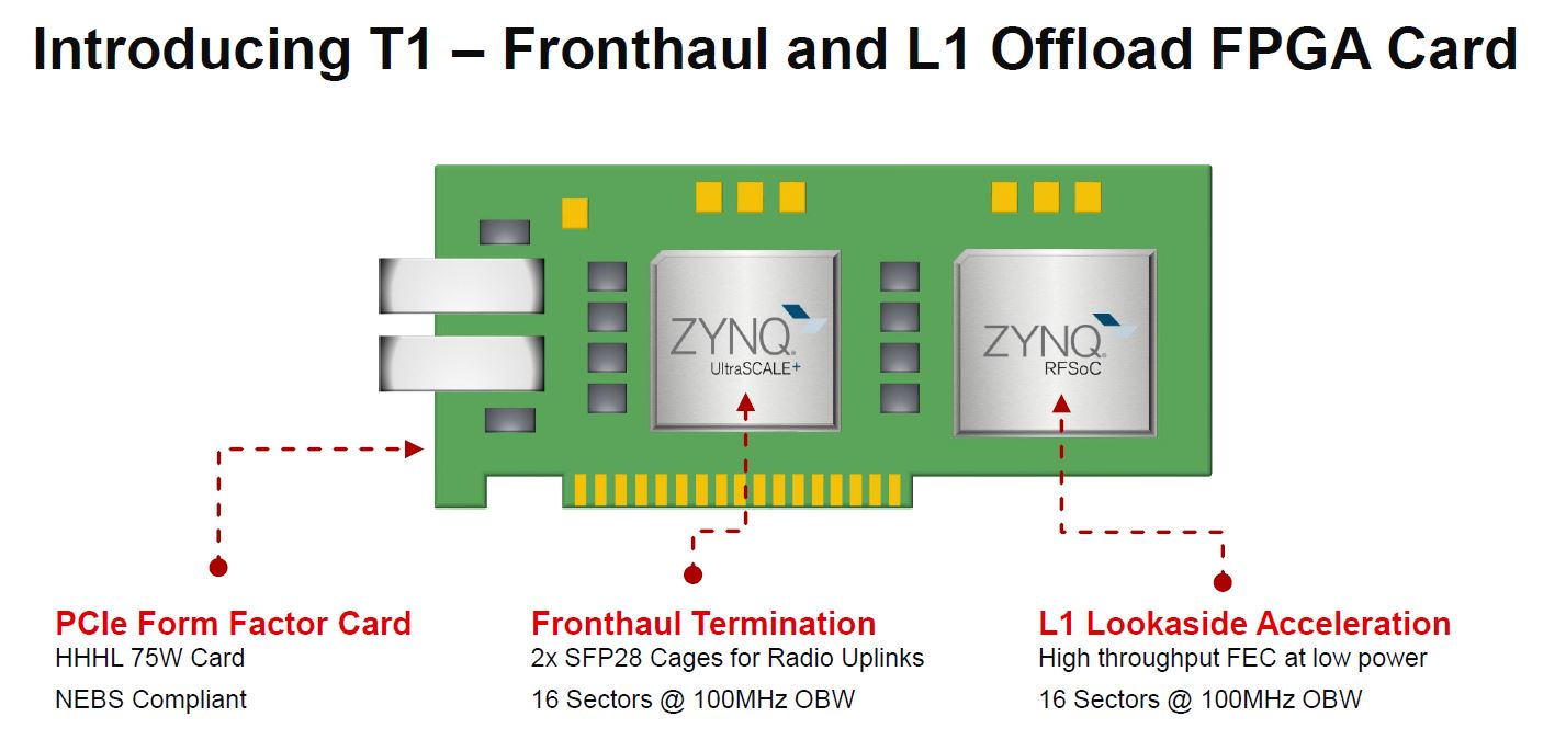
The Xilinx T1 effectively takes the fronthaul FPGA (Zynq Ultrascale+) and a Zynq RFSoC and puts them onto a 75W PCIe card so it can be installed in standard servers. The RFSoC has hardened logic for these baseband L1 functions. As a result, it achieves higher efficiencies than doing everything in FPGA logic gates and Xilinx hopes this means that its FPGAs are not replaced by ASICs in this role as quickly as they had been in the past.
Putting the two FPGAs onto a single card means that these cards can be added to commodity servers and scaled quickly to service more towers.
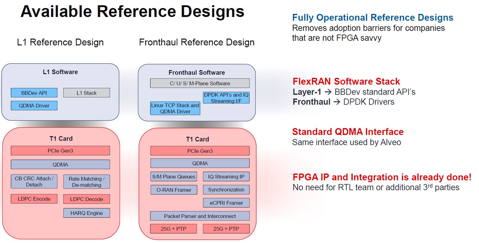
Along with the PCIe card, and its two FPGAs sharing the slot via PCIe bifurcation, the solution comes with reference designs and IP blocks that are ready out-of-the-box. A service provider does not need to start from scratch and can potentially use the T1 out-of-the-box using Xilinx and 3rd party IP. Xilinx sees this as more of a solution sale.
We asked and the card is a PCIe Gen3 card so we expect future versions to quickly scale to Gen4.
Final Words
In something of a twist for Xilinx, this is not a far-flung future product. Instead, it is a product that is already shipping. Normally, Xilinx announces product quarters or longer before they are available. It is also refreshing that Xilinx is bundling this as a solution with the IP blocks to turn it into a functional solution without needing to program and place logic. These are good trends for Xilinx.
Editor’s Note: I did mention to Xilinx on the call that “T1” in my mind is the name of an old-fashioned broadband line from the 1990s.


Dear Cliff,
A very good introduction to Xilinx T1 FPGA Card!
Could you please give me the best contact person (saleman) of this card in Xilinx?
Best regards,
Wen-Ping Lai
T1 also makes me think of the Automotive bidirectional twisted pair ethernet standards.. 1GBASE-T1 for example..
Comments are closed.