MikroTik CRS418-8P-8G-2S+5axQ2axQ-RM Internal Hardware Overview
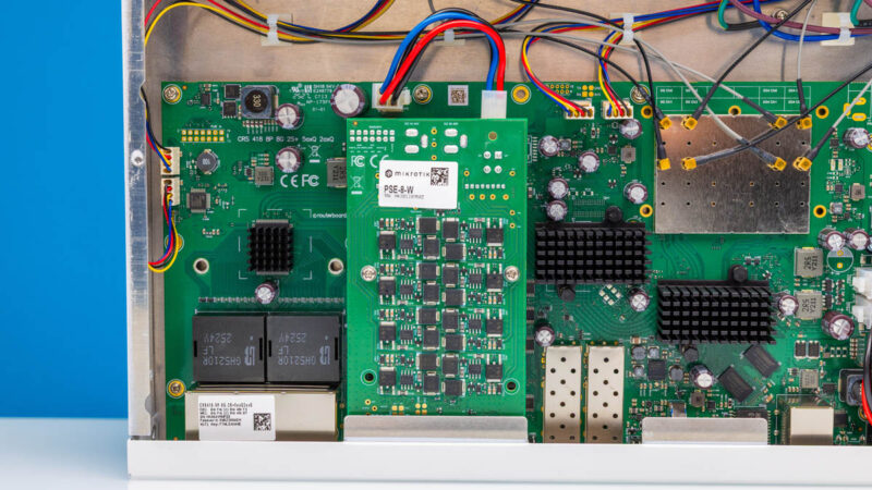
Inside, we can see a fairly neat layout. At the back of the switch, we have the power inputs and fans. In front of the switch, we have the switch PCB and the power supplies.
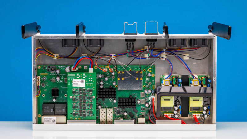
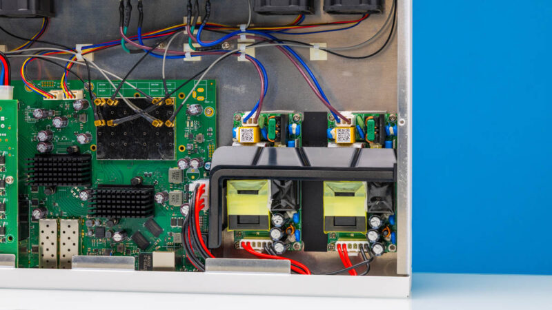
The 250W power supplies are in the front of the chassis. These are not hot-swappable, but a replacement part is available should you need it.
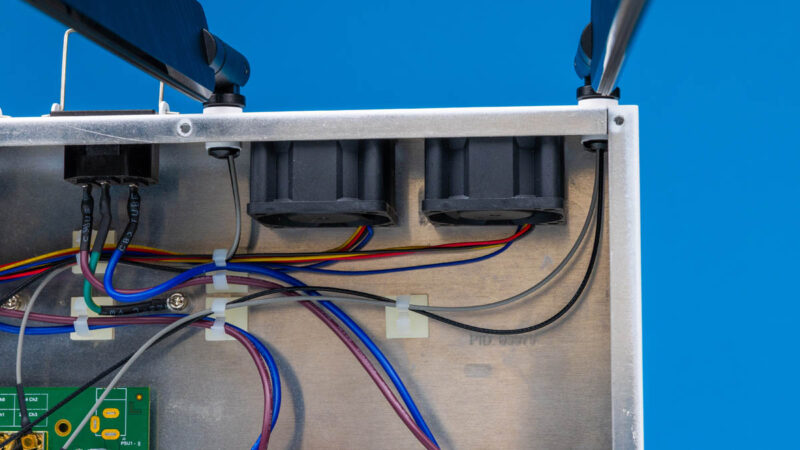
Inside, we also have the fans. Unlike some of MikroTik higher-end switches, these are not hot swappable.
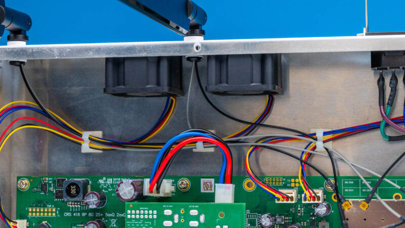
There are four fans inside, all connected via 4-pin PWM headers. We know some readers will think about fan swaps, but these are very quiet in practice thanks to distributing the cooling workload over a larger number of fans. In that respect this is a bit of a premium feature – a larger number of fans will cost marginally more to implement, but the payoff is in acoustics. That is a great trade-off in our book. Also, having more fans means that if one fails, there is still airflow through the chassis.
On the main switch PCB, you can see the WiFi radios. Unlike the non-WiFi model which has empty spots for these, this model has the WiFi hardware populated. You can see the Qualcomm QCN-5024 for 2.4GHz and QCN-5054 for 5GHz WiFi 6 radios. These provide 4×4 MIMO capability on both bands.
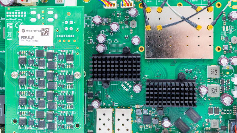
Often on these switches, we get only one switch chip plus possibly a few PHY chips. But this specific switch has more going on because of the Qualcomm chip. You can see the Qualcomm IPQ-8072A below the WiFi area. There are visible PCB traces to the WiFi radio area and DRAM packages just off to the side.
Above ports 9-16, we have the PoE+ board. This is a fairly common way to add PoE to switches that we have seen from a number of vendors.
Let us get to the block diagram to see how this is all connected.


1G ports come on its 2026 not 1996, yes still a lot of low bandwidth equipment that this will happily serve but for most people minimum 2.5G and really 10G when the price over capabilities and flexibility isn’t that much. 16x10G ports may be enough for a lot of SOHO or home labs and the SFP’s for expansion.
For who is this device made? Why add wifi to it? I don’t see the target audience at all.
L3 hardware feature support: https://help.mikrotik.com/docs/spaces/ROS/pages/62390319/L3+Hardware+Offloading#L3HardwareOffloading-CRS3xx:Switch98DX3xxxand98DX2xxxSeries
I’ll repeat my question from the non-WiFi model review. Have you turned on the L3 HW offload on the switch when testing routing?
“Next, there are two more Ethernet ports. One is the console port…”
I seriously doubt that’s Ethernet. I’d expect that to be the Cisco-style serial over RJ45 mentioned in the block diagram.
Did you try it?
My guess is that the target audience for the WiFi is for admins to have WiFi access when in the network room, rather than burning a port for an access point. However not having some 2.5Gbps ports makes it somewhat less interesting.
Great overview of the MikroTik CRS418?8P?8G?2S+5axQ2axQ?RM! I liked how it combines a 16?port 1GbE switch, two 10G SFP+ uplinks, PoE+, and dual?band Wi?Fi?6 with 4×4 MIMO—all in one compact router.
Nice overview of the MikroTik CRS418?8P?8G?2S+5axQ2axQ?RM. I liked how you highlighted the PoE+ ports plus the added Wi?Fi?6 with 4×4 MIMO—sounds like a handy all?in?one box for small networks and great value.
Thanks for the review of the MikroTik CRS418 with PoE+ and Wi?Fi?6. I liked how you explained the Qualcomm CPU and dual?band 4×4 MIMO—sounds like a solid all?in?one for small networks.
Great review! I liked how you highlighted the combo of PoE+, the Qualcomm CPU, and Wi?Fi 6 dual?band 4×4 MIMO. Sounds like a versatile all?in?one for small networks. Thanks! Really appreciate it!
Thanks for sharing this review of the MikroTik CRS418-8P-8G-2S+5axQ2axQ-RM. I liked how it combines a PoE+ switch, router, and dual?band Wi?Fi?6 in one box—very handy for home or office use.