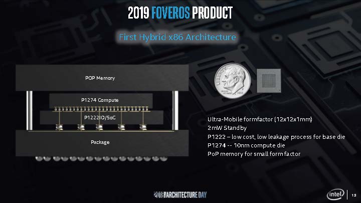
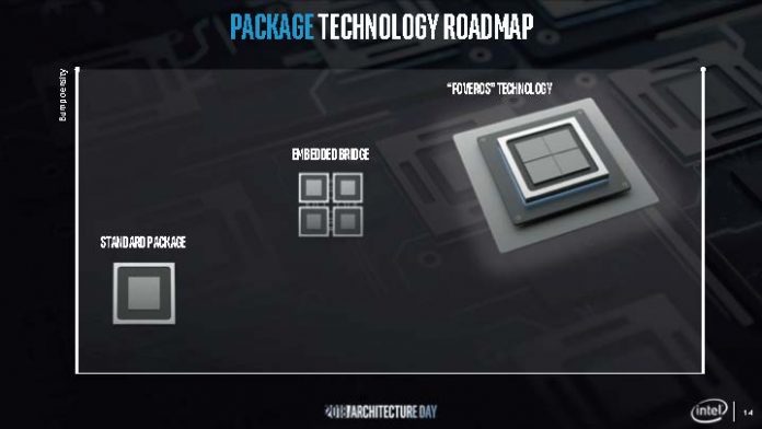
The future of high-end processors we use in servers and even in the embedded edge is multi-die. AMD has been exploiting multi-die technology in its EPYC and Ryzen parts. With the 7nm generation of each releasing in Q3 2019, Intel’s monolithic die days are numbered. Although Intel touts monolithic die technology, it is already gluing together chips with Intel Agilex FPGAs and EMIB as well as at the edge with Intel Foveros. Today, Intel is announcing the next-generations of its co-packaging technology called Co-EMIB and Intel Omni-Directional Interconnect.
Intel Co-EMIB
If you were wondering what you get combining EMIB chip-to-chip bumps and Foveros chip stacking, the answer in the short term is Co-EMIB. Foveros is used to build the main elements of a chip. EMIB is then used to tie those elements together.

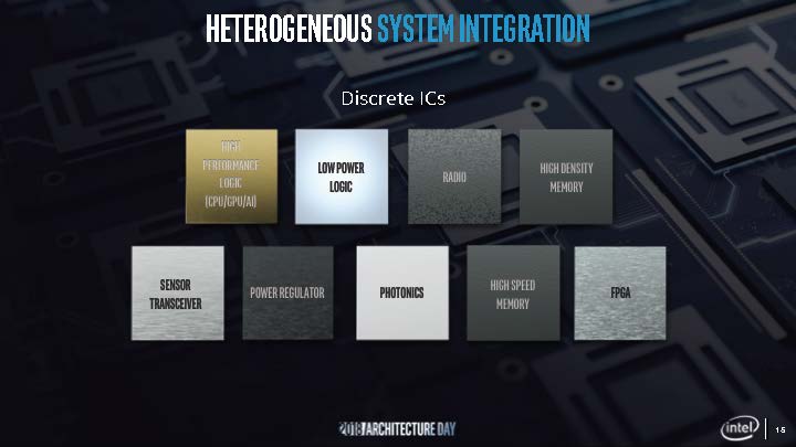
The industry is struggling with how to build different logic elements on the best process for each. Analog may, for example, be better suited to an older process than the primary CPU or FPGA cores. By using different die built on different processes, the company can create integrated chips that take the best from each.
Intel Omni-Directional Interconnect
Beyond Co-EMIB is Intel Omni-Directional Interconnect or ODI for short. Here, the top chip of each package can communicate on a horizontal plane with other chiplets. This is similar to how EMIB works today. It can also communicate vertically through large Through-Silicon Vias (TSVs) in the base die below. That is similar to today’s Foveros. ODI also has large vertical vias to allow power delivery to the top die directly from the package substrate.

Intel says that these vertical vias are larger and offer lower resistance. As a result, they can deliver more power to chips above. They can also offer high bandwidth, low latency paths between chips and the package substrate.
In its ODI announcement, Intel specifically called out data center workloads, such as AI and supercomputing. So that is a hint on where that may be headed first.
Intel MDIO for Chiplet Interface
Along with the Co-EMIB and ODI announcements, Intel is also talking MDIO. MDIO is the company’s protocol interface between chiplets that will replace the current AIB interface. The company says that MDIO doubles the pin speed and bandwidth over AIB which is important if you have a roadmap full of glued together chips. Intel MDIO is slated for 2020 release.
Final Words
For server buyers, here is the key takeaway. While Intel is strongly behind monolithic die designs today on the Xeon side, this is not where we are going. In the next few years, the majority of chips you buy will be multi-chiplet designs. AMD was the first company in modern times to go this direction, but Intel is all-in on not just matching AMD’s design vision, but also innovating on the packaging to leapfrog. Looking ahead to 2020 and beyond, Intel ODI and MDIO are going to be the next steps in that process.


When will you guys be doing a performance review of Ryzen 3900X? All the “hardware” sites think a proper test of a CPU is to run a game as fast as possible at very low screen resolution. We need some real numbers about real applications!
Love the (deserved) jab at Intel “if you have a roadmap full of glued together chips”.
Seems like glueing chips together isn’t such a bad idea after all.