
We are here at the Intel Foundry Direct Connect 2025 event in San Jose, California, for what is really a make-or-break day for Intel. Intel needs the Intel Foundry business to start taking off, and we are approaching the launch of Intel 18A. Today, we hope to hear more about Intel 18A progress, as well as more updates on the future roadmap, as we heard last year.
This is being done live so please excuse typos.
Intel Foundry Direct Connect 2025: Make-or-Break Time For Intel
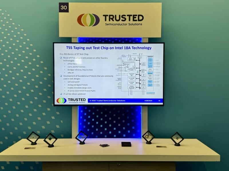
Something I noticed walking in is that there were customers talking about working with Intel 18A. Trusted Semiconductor Solutions is focused more on the defense industry than the consumer and data center space as an example.
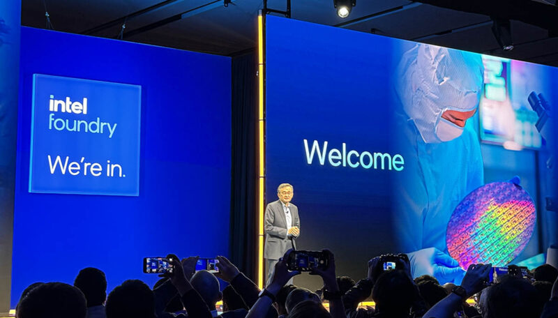
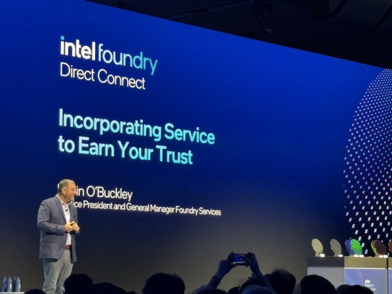
The event started with an address by Lip-Bu Tan in his fifth or so week as Intel CEO.
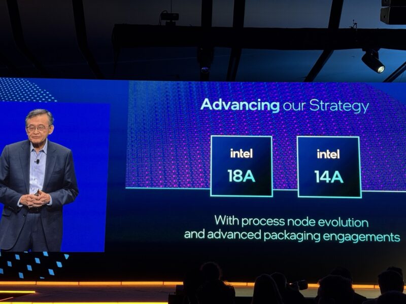
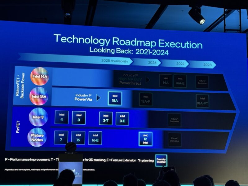
Panther Lake is going to be the launch vehicle for Intel 18A and is slated for 2025. Clearwater Forest has been pushed to 2026.
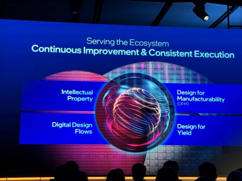
Intel has four pillars for serving the foundry ecosystem including intellectual property, design for manufacturability, digital design flows, and design for yield.
Synopsys got on stage and is discussing working on the Intel PDK and 18A and 14A for its IP development. Synopsys says that Intel has been making “tremendous progress” ramping how it works with others.
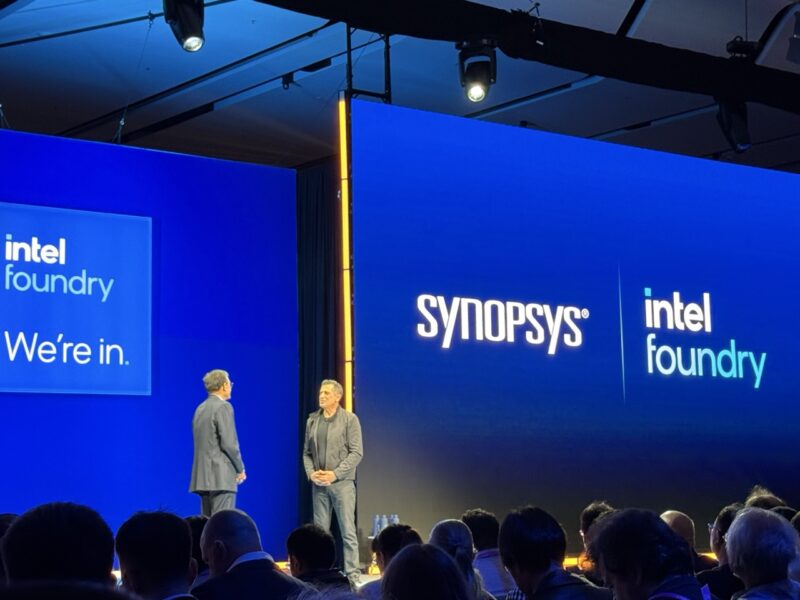
Synopsys says in Intel 10nm it would be more than twice as much effort than industry standard (TSMC.) Now, Synopsys says it is on parity with industry norms.
- New certified AI-driven digital and analog design flows for the Intel 18A process node, as well as production-ready EDA flows for the Intel 18A-P process node with RibbonFET gate-all-around transistor architecture and PowerVia backside power delivery.
- Of note, Synopsys was uniquely involved in early Design Technology Co-Optimization (DTCO) for Intel 18A to enhance PPA, and is engaged in early design technology co-optimization for Intel 14A-E?today.
- New collaboration to enable Intel’s EMIB-T (EMIB using TSV) advanced packaging technology with an EDA reference flow powered by Synopsys 3DIC Compiler and support with Synopsys IP.
- Founding member of the Intel Foundry Accelerator Chiplet Alliance, building on our strong track record of delivering breakthroughs in multi-die design technology (e.g., we previously collaborated on the world’s first Universal Chiplet Interconnect Express (UCIe) interoperability test chip). (Source: Synopsys e-mail to STH)
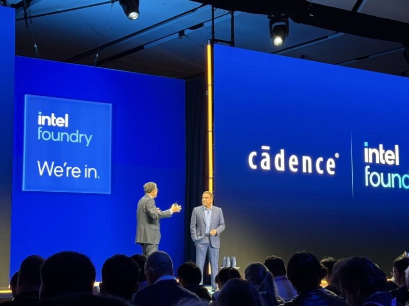
Cadence is on stage next talking about using AI in EDA workflows. Cadence is also talking about how Intel has very good packaging technologies as well as backside metal technologies. As an interesting nugget in 14A something that will change is that assuming that the dies will be put into some kind of advanced packaging.
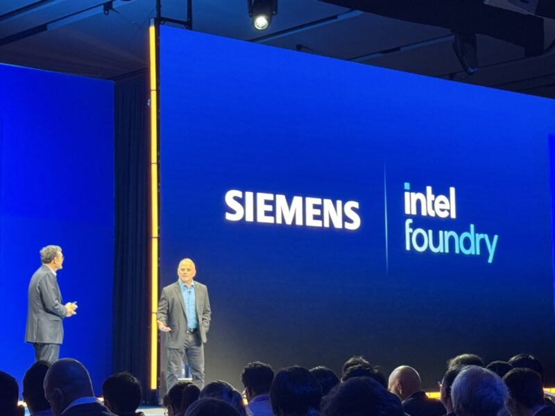
Siemens EDA is on the stage talking about how it is working with Intel and bringing their design for manufacturability flows into production with EMIB and other technologies for advanced manufacturing.
Not lost on me at this point is that we are talking tools, not customers or roadmap at this point.
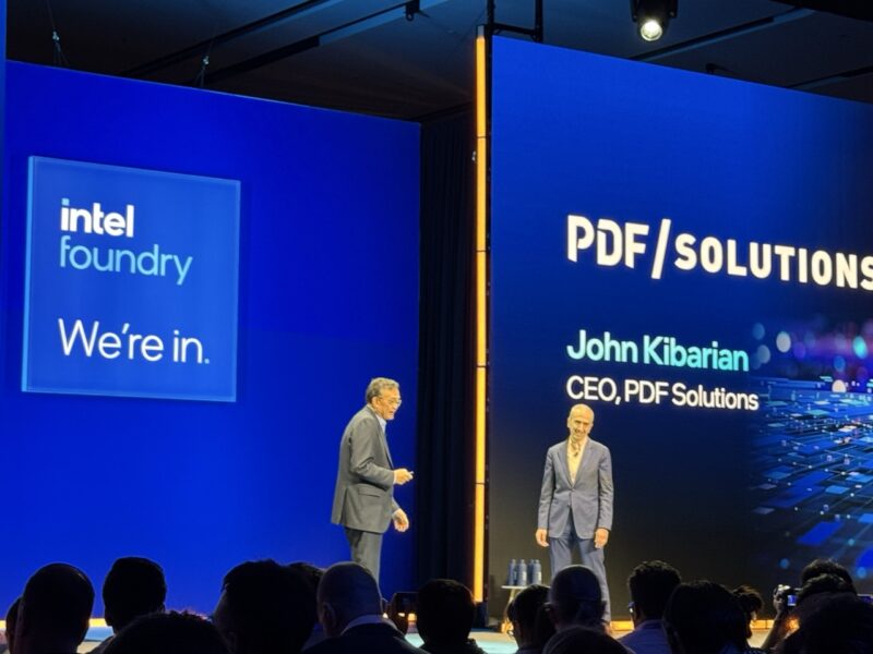
Next we are talking about design for yield with PDF/Solutions. This partnership is to help not just Intel’s internal products (Intel started using PDF years ago) but also for working on the processes for external R&D teams. The goal, of course, is to ensure that processes and designs yield as high as possible.
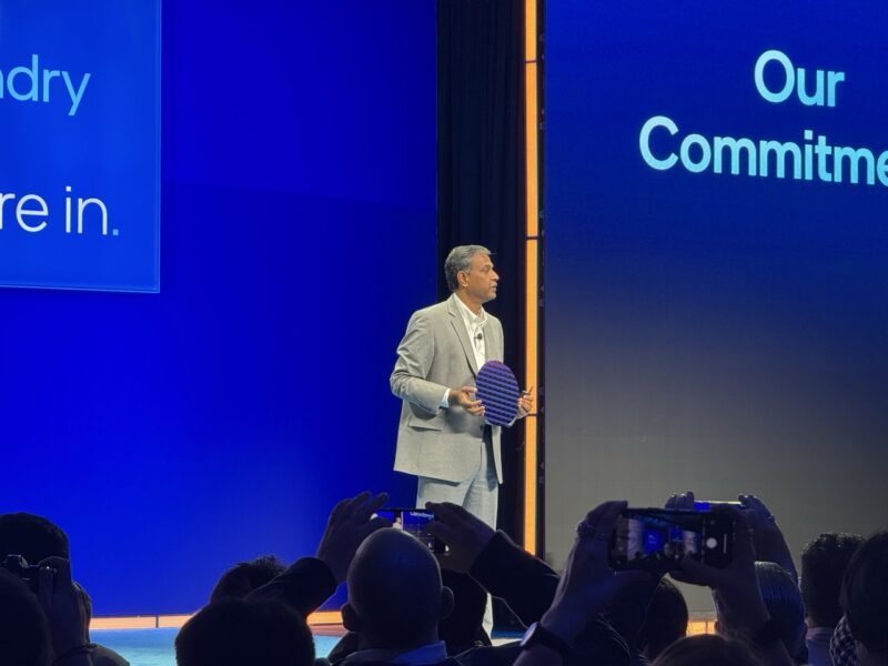
A wafer has arrived on stage! Dr. Chandrasekaran’s talk is opening with building trust with ecosystem tools and IP, customer service and predictable execution, and having the right technology and global capacity.
Intel has been making investments in technology and capacity.
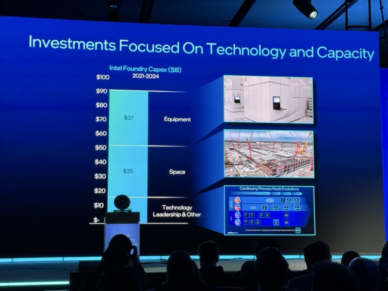
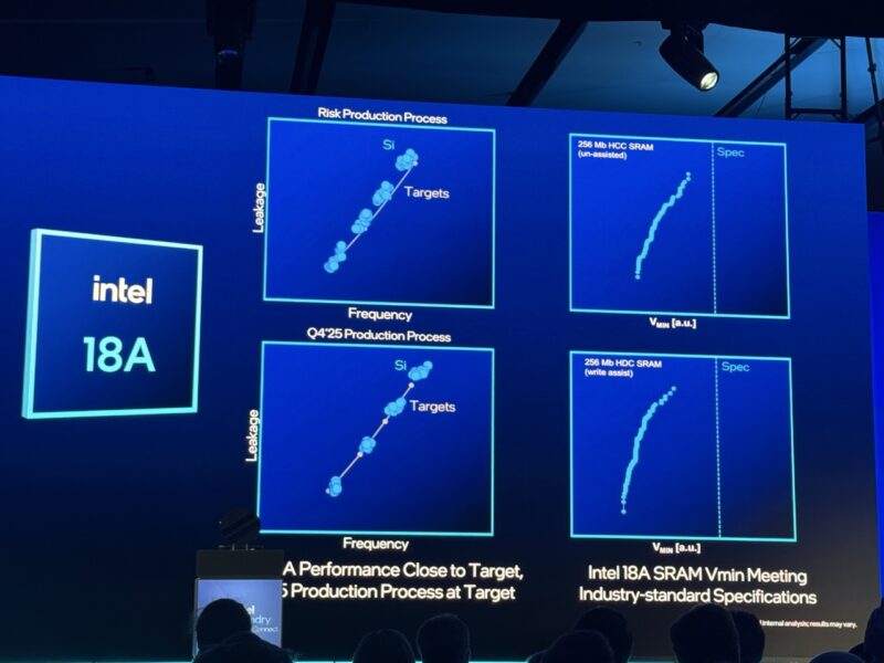
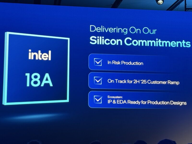
Here is the history from 2021 to 2025 as Intel focused on fixing its technology capabilities. 18A is now in risk manufacturing.
Intel has many sites around the world for manufacturing.
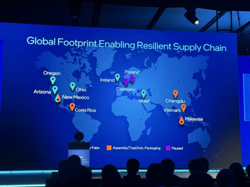
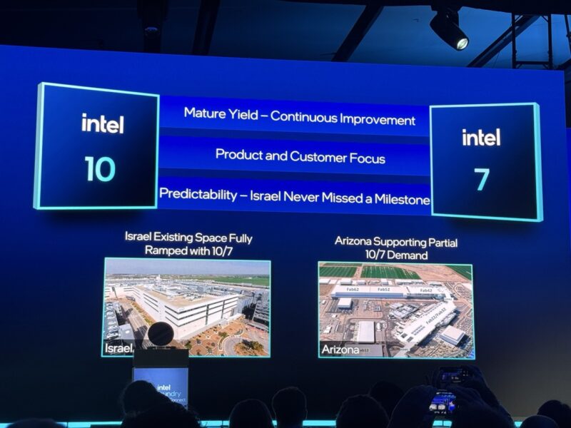
In Israel and Arizona, Intel has mature Intel 10 and 7.
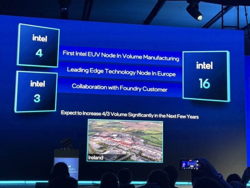
Intel discussed the EUV nodes and how it had to evolve from copy exact. It also discussed how it has been working with Mediatek.
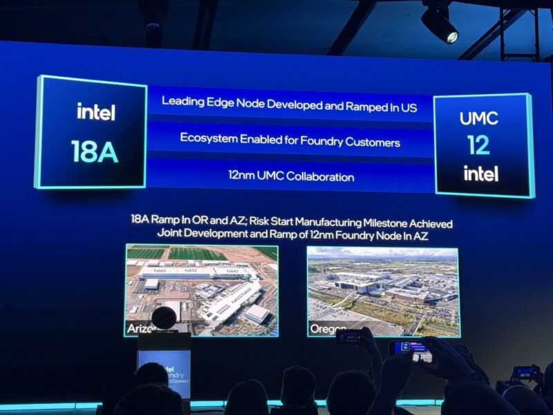
Now Intel is highlighting Arizona (only a few minutes from STH’s studio.)
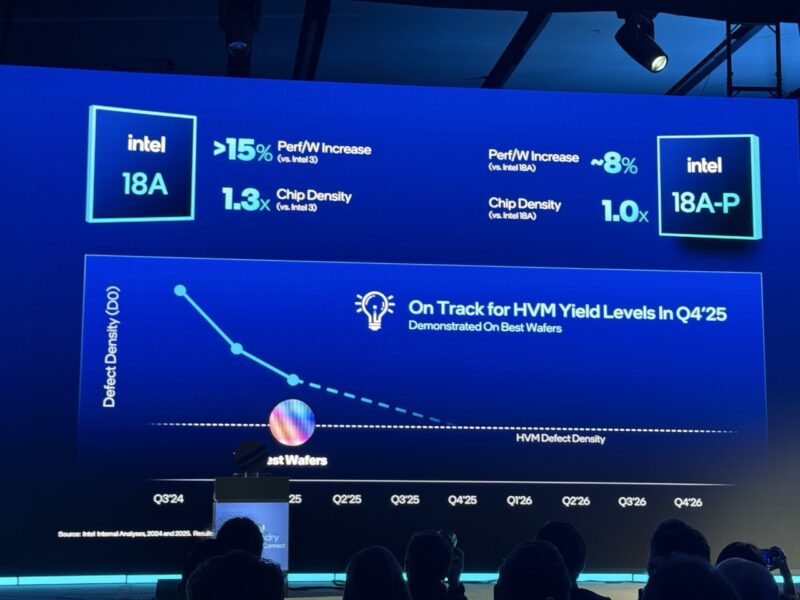
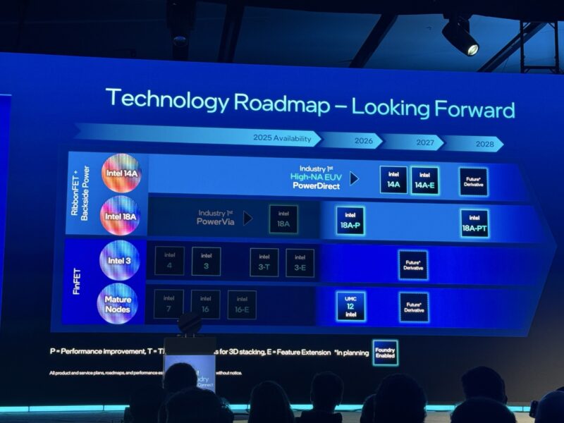
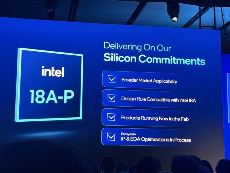
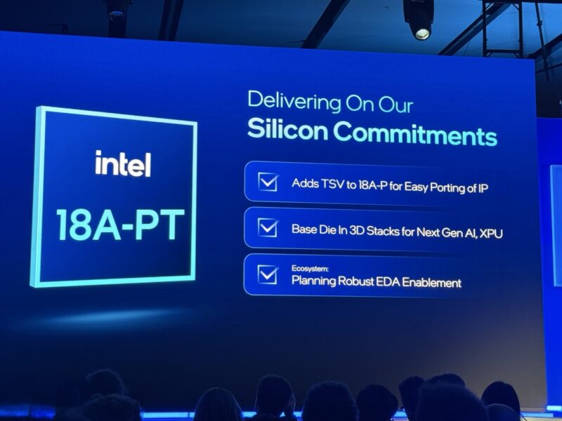
Intel 18A will also have an Intel 18A-P variation, and eventually 18A-PT.
Intel 18A expected to hit high volume manufacturing in late 2025 based on some of the key process improvement programs that Intel is working on.
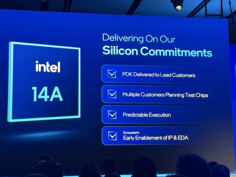
Intel is now focusing on 14A, and it is being run in Oregon today. Here is the roadmap going into 2028.
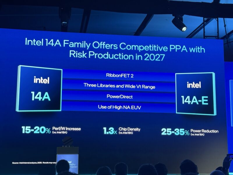
Intel says that Intel 14A will be a 15-20% performance per watt increase and bring second generation technologies including the RibbonFETs.
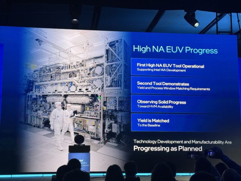
Intel has a second high NA EUV tool operational working on Intel 14A already. This tool came up much faster than the first one.
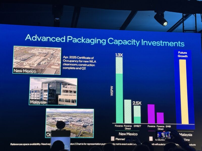
Intle is also talking about its advanced packaging solutions in places like New Mexico and Malaysia.
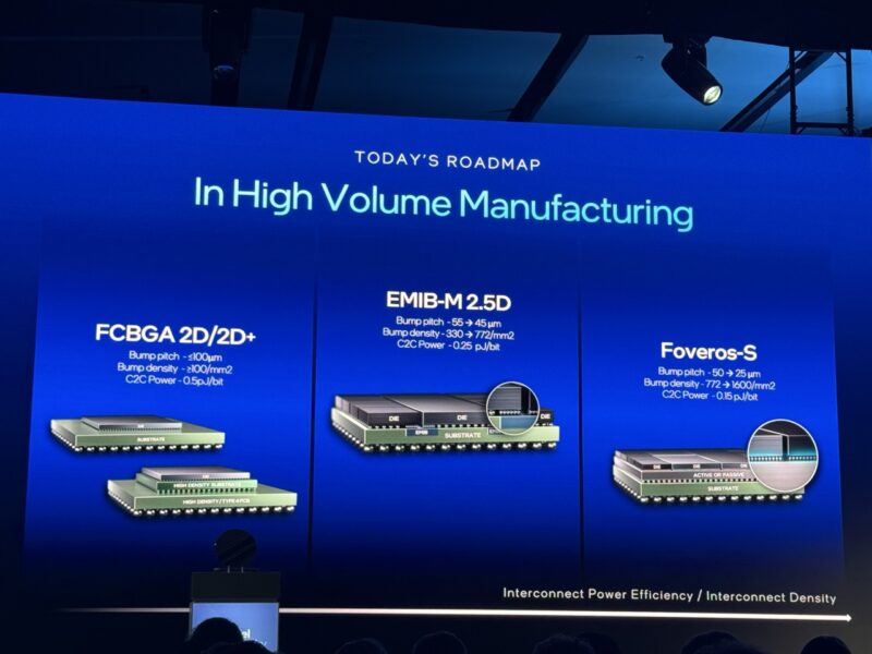
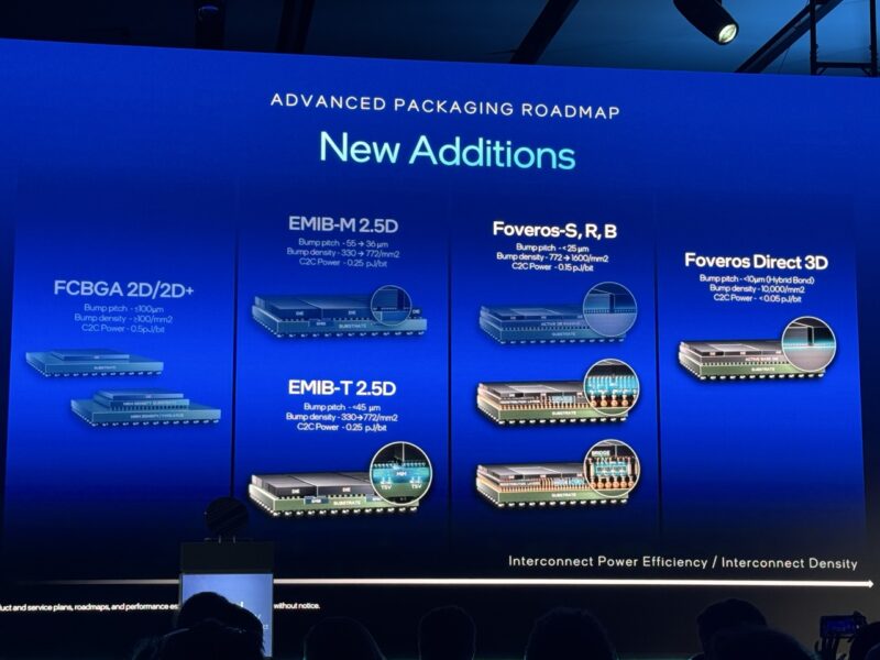
There is more though. Intel has new technologies like TSV with EMIB for EMIB-T, and a new lower cost Foveros.
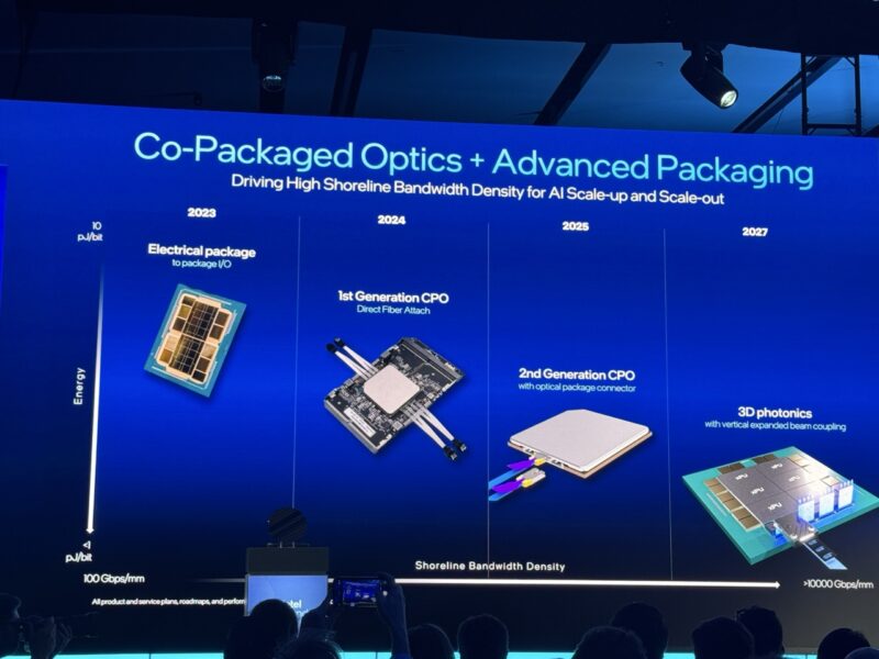
Intel is also talking about more co-packaged optics. Of note, the 2nd Gen CPO looks a lot like what we saw in 2022.
Intel showed its current capacity in locations, but also where it can grow. Intel says in 6-8 quarters it can increase capacity at current sites.
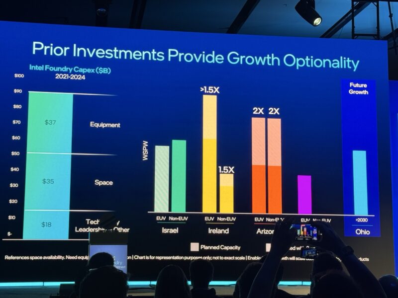
Beyond wafer manufacturing, Intel also has packaging capabilities and headroom to grow operations.
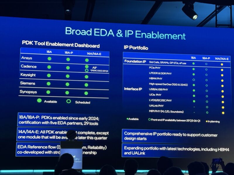
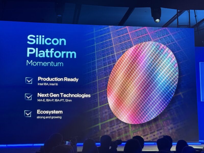
Intel says that its tooling is on track for 18A and 18A-P and it is working on 14A enablement now.
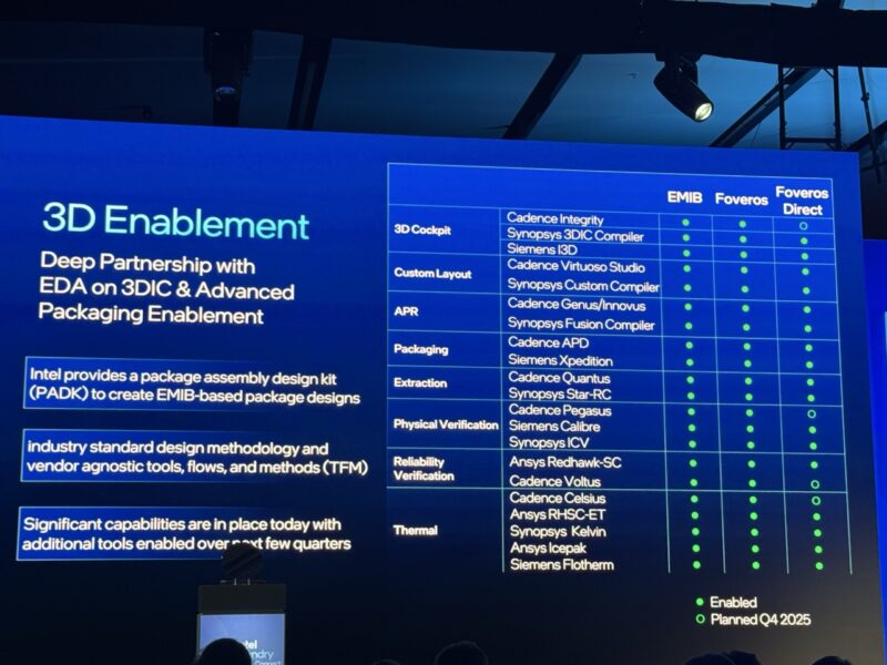
Here is the 3D packaging enablement look.
Intel says it is using Boston Dynamics robots in fabs for consistent monitoring.
Intel also brought out an Intel 14A wafer run in Oregon on stage.
It looks like it is Kevin’s time on stage as they are bringing out a lot of wafers (but to the wrong side of the stage as they are opposite me!)
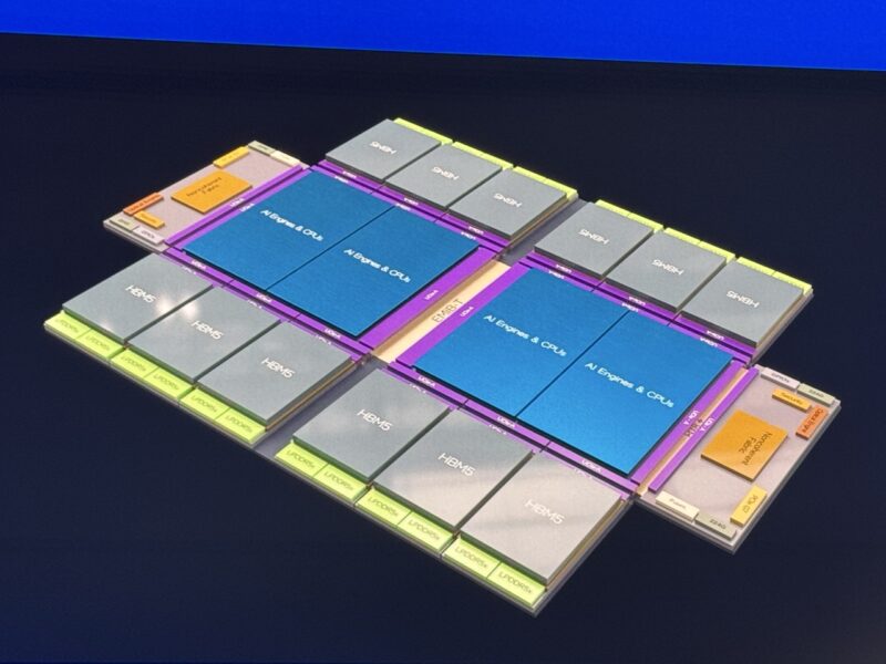
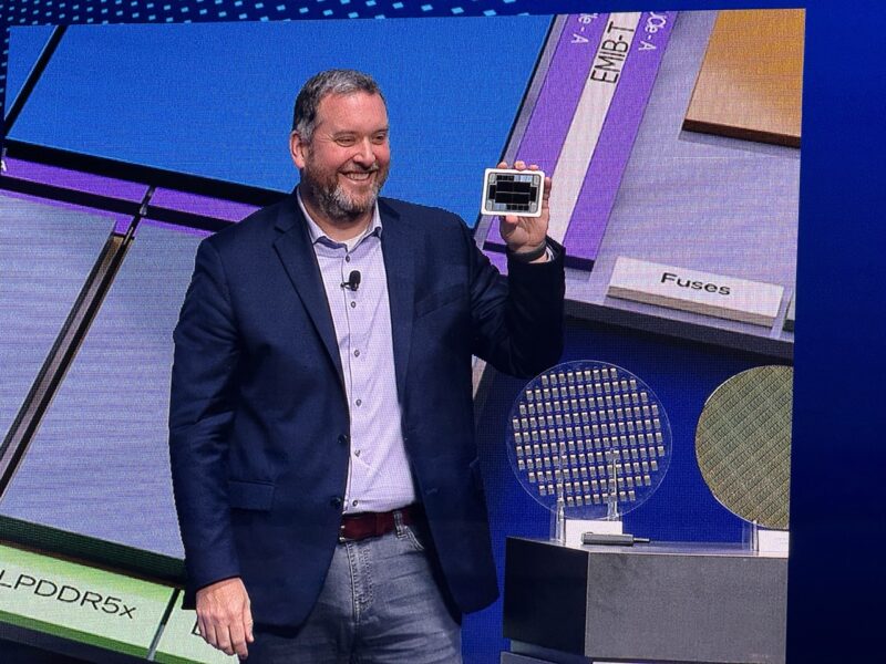
Intel is showing a future 12x reticle chip with AI engines, high-speed interconnects, HBM5, and LPDDR5x, PCIe Gen7, optical engines, UCIe-A, EMIB-T, 224G PHYs, sucurity blocks and more.
Intel 18A is on track for production this year.
Intel 18A-P is focused on a different optimization curve for broader market applicability.
Intel 18A-PT adds TSV for high-end chips. This is what Intel believes is going to be leading process for large AI chips when it arrives.
Intel 14A is coming with second generation technologies.
Intel said on the mature node side that Intel 16 has not just a MediaTek chip tape out, but it is a design now going into production. Intel is also working with UMC on the UMC 12nm line in Arizona. Intel is also thanking the US Government and suppliers for secure end-to-end development to production capabilities in the US.
Now Kevin is going into the advanced packaging and how this is required for next-generation chips.
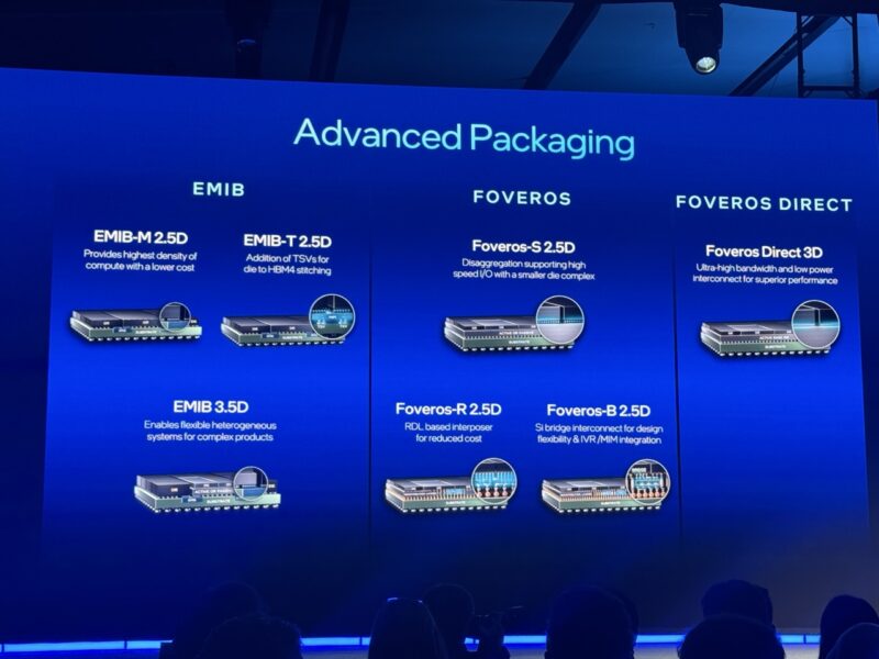
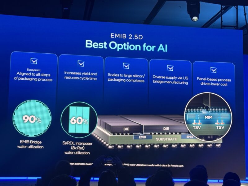
Intel is discussing EMIB 2.5D as an alternative to large silicon interposers since it can cut the manufacturing time by weeks.
Intel has Amkor on stage discussing how it is enabling EMIB for partners. Amkor says it will be bringing advanced packaging to Arizona to augment exiting South Korea and Portugal sites.
That ~12 reticle size package diagram from earlier, here it is in a package. Very cool.
All good stuff from Intel today.
Final Words
The morning keynotes are done, and Intel did exactly what it needed to do. The key themes seem to be: Intel’s new technology both on process and packaging is on track, and it is working with partners to develop an ecosystem for non-Intel Products customers. Intel also leaned into its ability to manufacture in the US and is touting itself for supply chain diversity. A lot of this also seems to hinge on 18A going well. I cannot wait to see those products hit our lab.


Just curious if intel can get the foundry working which is looking promising do you think there would be any benefit in back-porting technologies like Backside power delivery (BSPDN) to there mature nodes? As well as maybe creating a pdk for there 7/10 nodes or a derivative like an intel 6 or 8?
I know not all designs benefit from BSPDN but surely there are some that would and it could give them a competitive advantage over TSMC or Samsung who don’t have that yet. Not to mention for intel 4 (which if I recall correctly is very similar to if not design rule compatible with intel 3) they already have a BSPDN work mostly done and have shown working chips with it years ago.
I know that they probably wouldn’t have those PDK’s available and that TSMC and Samsung to a lesser degree already have nodes out there but if those nodes are anything like Globalfoundries nodes in longevity they may have some long term revenue potential?
Comments are closed.