
At Hot Chips 30 IBM POWER9 took center stage during a talk that centered around the company’s transition to serialized interconnects. Recently we covered that the new IBM POWER9 E950 and E980 Servers Launched. At the show, the company explained their vision for scaling up memory in a server and providing high speed interconnects.
Scale-Out v. Scale-Up IBM POWER9
IBM offers its chips in multiple configurations. One is a scale-out design the other is the scale-up design. First, take a look at the common features.
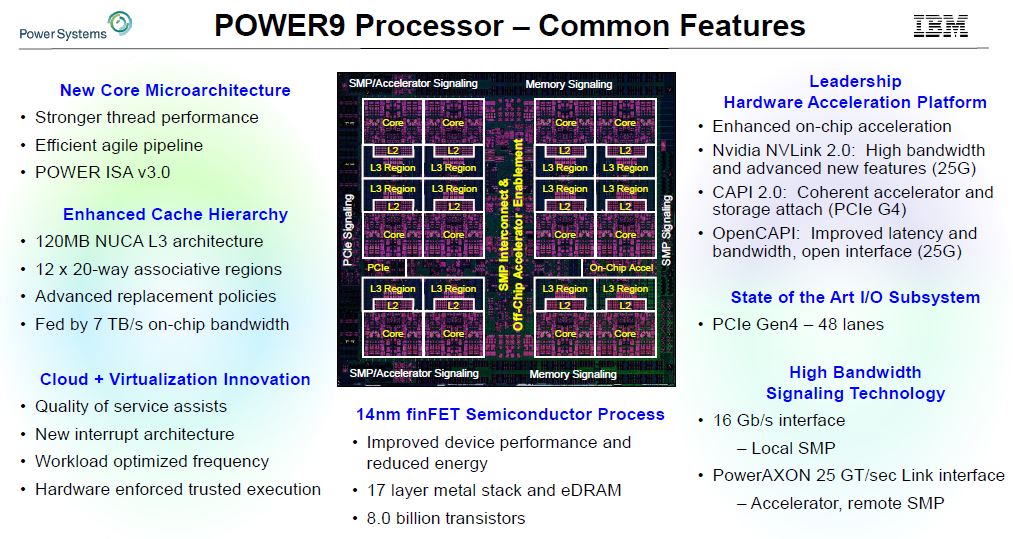
These are massive chips. They incorporate huge L3 caches, cores that in the scale-up CPUs have 8-way SMT. L3 cache is provided by eDRAM as the cache sizes have grown. IBM POWER9 has supported PCIe Gen4 since its introduction while we are not going to see x86 from AMD then Intel supports PCIe Gen4 until later in 2019.
Focusing on the memory, the Scale Out design uses direct attach DDR4 ports. It is not in the slides, but this is like how the Intel Xeon Scalable, AMD EPYC, Cavium ThunderX2 and others support DDR4. The DDR4 memory controllers are in the CPU silicon.
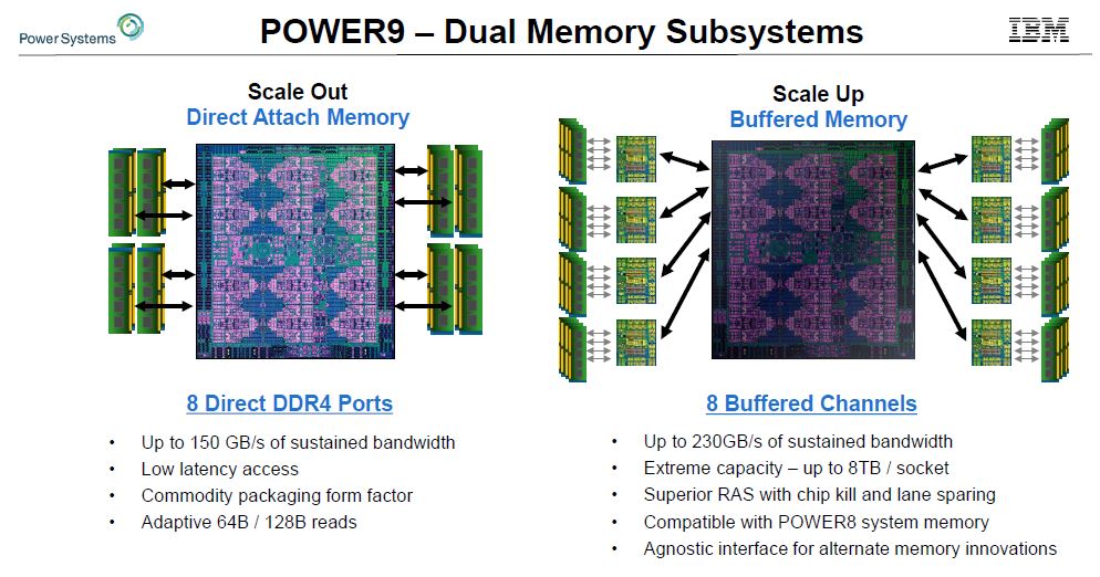
For the IBM POWER9 Scale Up design, the company uses a serial interface to buffer chips. This means they can support eight buffer chips. These buffer chips can, in theory, be used for different types of memory including GDDR5/ GDDR6. Each of the current generations has four channels so it was casually dropped on stage that they are getting 32 channel DDR4 (via 8 buffer chips) on their POWER9 Scale Up design. That is a big reason They are able to handle 4TB RAM per CPU.
Another side effect is that the serial interfaces are smaller on the die than the DDR4 controllers. Scale Up designs that use edge area for off-die I/O can fit more PowerAXON (more on this in a bit), and address more memory. You will also notice that in the diagram, and in our briefing IBM confirmed, that the Scale Out designs have some wasted edge space.
We should note, Intel during their talk at Hot Chips 30 spoke on this subject and noted it was a significantly more costly way to build memory.
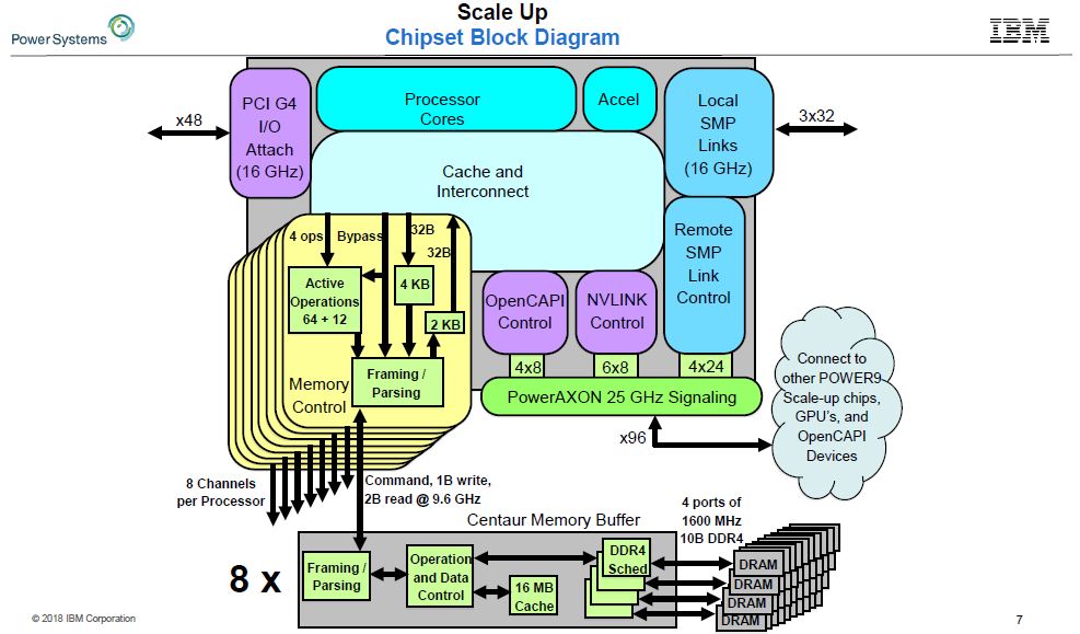
IBM PowerAXON For SMP, OpenCAPI, and NVLink
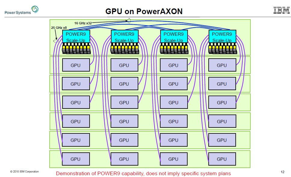
The focus on more generalized I/O implementation does not end there. Although POWER9 has 48x PCIe Gen4 lanes, it also has technology the company calls IBM PowerAXON. PowerAXON is a 25GT/s interface that the company sees scaling in the future to faster speeds. IBM calls its SMP CPU to CPU links A and X. The same I/O block has IP for OpenCAPI (the O.) Finally, as we saw with the US DoE Announces Summit with IBM Power and NVIDIA Tesla, PowerAXON can also speak native NVLink. This is different than x86 servers that go PCIe to GPU then GPU to NVLink.
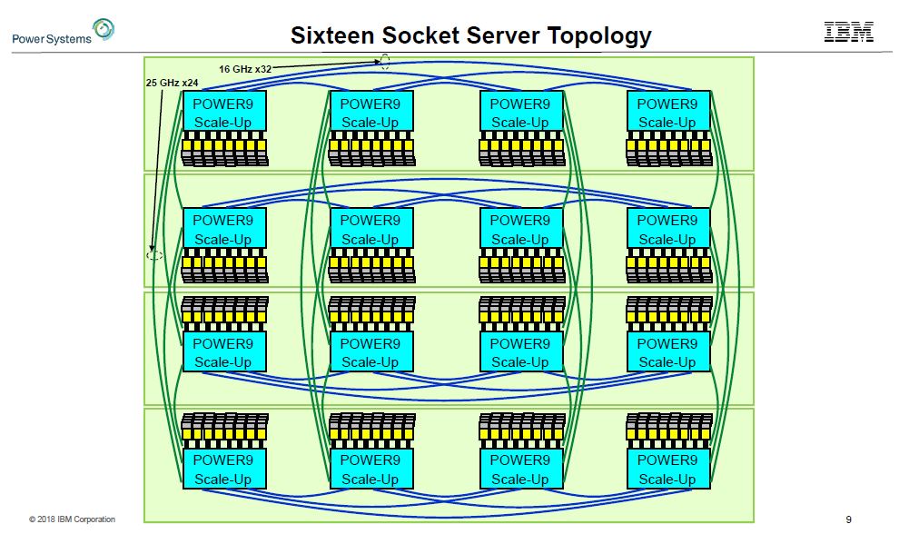
The A and X links in the PowerAXON can be used to connect to a sixteen socket server topology. Each CPU can connect to six other CPUs directly which is far more than we see on the x86 side with current chips limited to two or three direct connections. This is why IBM is simply able to out-scale x86.
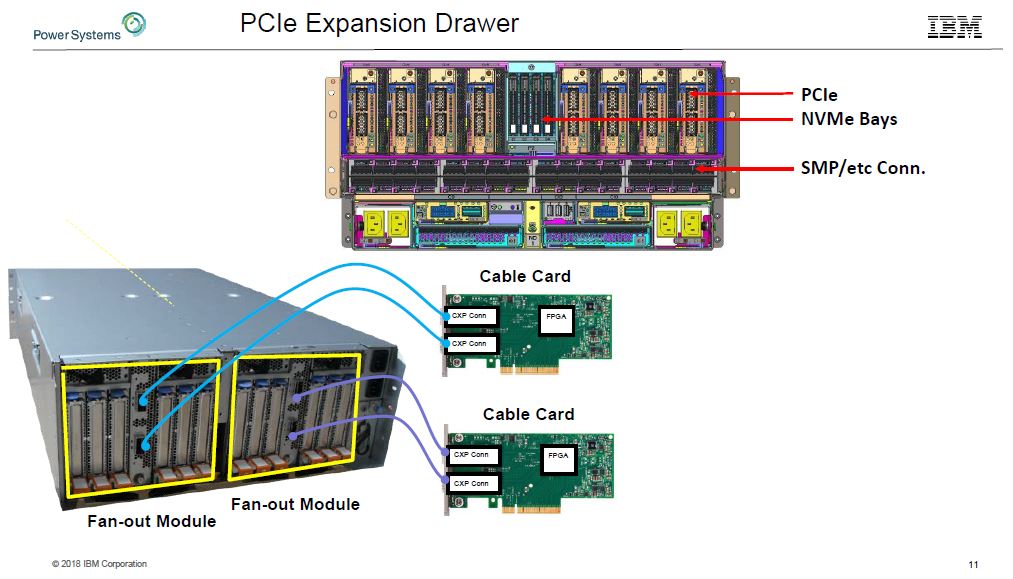
On the basic PCIe side, the servers can have external PCIe 4.0 cabling to connect a multitude of devices.
When it comes to deep learning, AI, and HPC, the quad POWER9 Scale Up server does not need PCIe to attach to GPUs. Instead, it can use NVIDIA NVLink to directly attach each CPU to six GPUs.
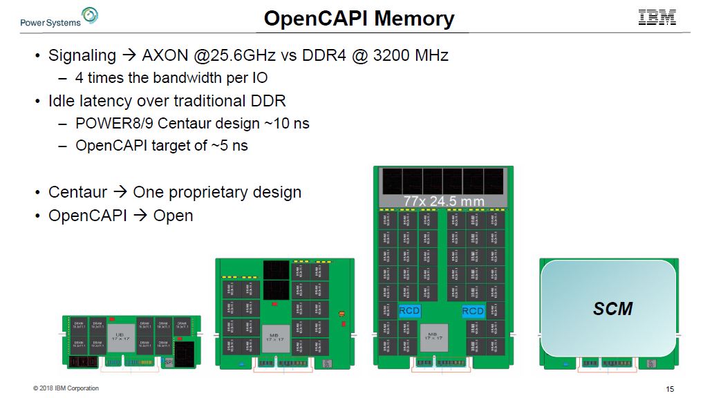
The industry knows that it needs to move to higher-speed interconnects and the traditional model will not work. PowerAXON can also connect to OpenCAPI memory. This can be a normal DDR4/5 memory. It can also be higher-end designs for fault tolerance.
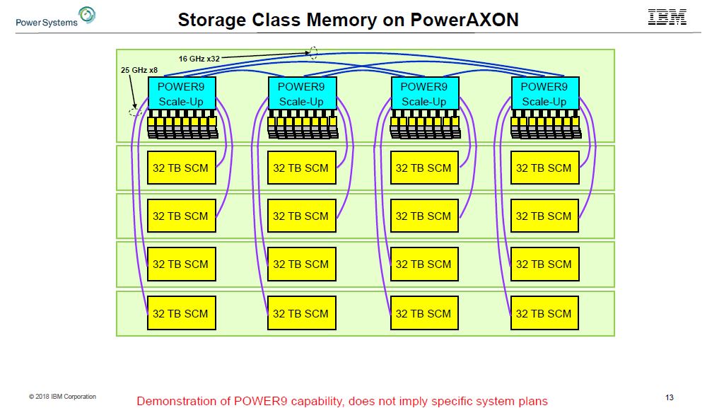
One other potential design IBM showed off was adding storage class memory using the O in PowerAXON for OpenCAPI. If a 16TB quad socket server is not enough, IBM can see this technology scaling well beyond 16TB for larger datasets without having to go to the slower PCIe bus or the fabric.
The quick summary is that if you need a big system today, and want IBM reliability, the company has you covered so long as you have the budget.
IBM POWER9 Roadmap
At the conference, IBM also spoke about their roadmap. Here is the currently proposed roadmap:
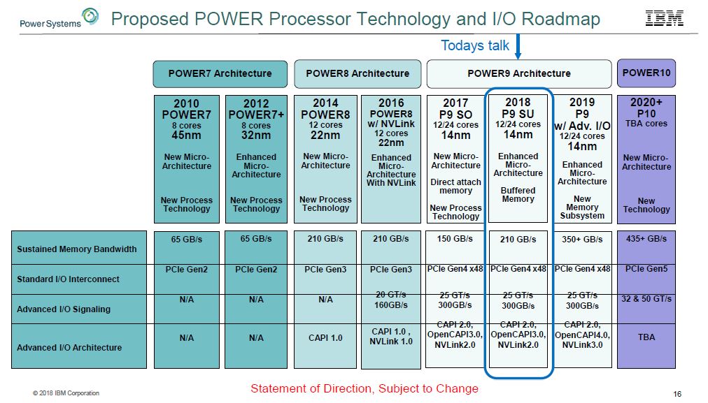
Looking on the roadmap, the company has plans to bring in the POWER10 type memory subsystem (buffered) into POWER9 next year in a new update.
Here is the big one on the roadmap that apparently a lot of people just missed. NVLink 3.0 is in the 2019 swim lane. Since the NVIDIA Tesla P100 “Pascal” generation has NVLink 1.0 and the NVIDIA Tesla V100 “Volta” has NVLink 2.0, this confirms that IBM is planning to support NVLink 3.0 for next-generation NVIDIA data center GPUs in 2019.
Final Words
Overall, the IBM POWER9 is just cool. We have another quad socket x86 (Xeon Platinum) review in the publishing pipeline, and we also have Intel-based 8x NVIDIA Tesla GPU systems that you may have seen for our deep learning series. We wish we could use the IBM POWER9 versions of these systems, but alas, they are out of our budgets for site content.
The NVIDIA NVLink 3.0 is not announced by the company and is on IBM’s proposed roadmap. However, we think it is safe to assume that NVIDIA will follow-up the wildly successful Volta program with a new high-end Tesla chip. We also think it is likely that NVIDIA will continue to expand its technological lead with the NVLink interconnect to a new generation. NVIDIA is investing heavily in NVLink including making its own switch chips that we highlighted in NVIDIA NVSwitch Details at Hot Chips 30. There is a good chance that we will see NVIDIA NVLink and a new Tesla flagship GPU in 2019.


Yea but they’re crazy expensive and that’s why web 2.0 happened on scale out.
good nvlink 3.0 catch STH. you’d think IBM is big enough that they’d have lawyers check public slides for that
I think this geometry dash meltdown idea is definitely interesting.
nice nvlink 3.0 capture STH. You would think IBM would be large enough to have attorneys look for that in public slides.
Yes, but they are prohibitively expensive, which is why Web 2.0 emerged on a larger scale.
Comments are closed.