
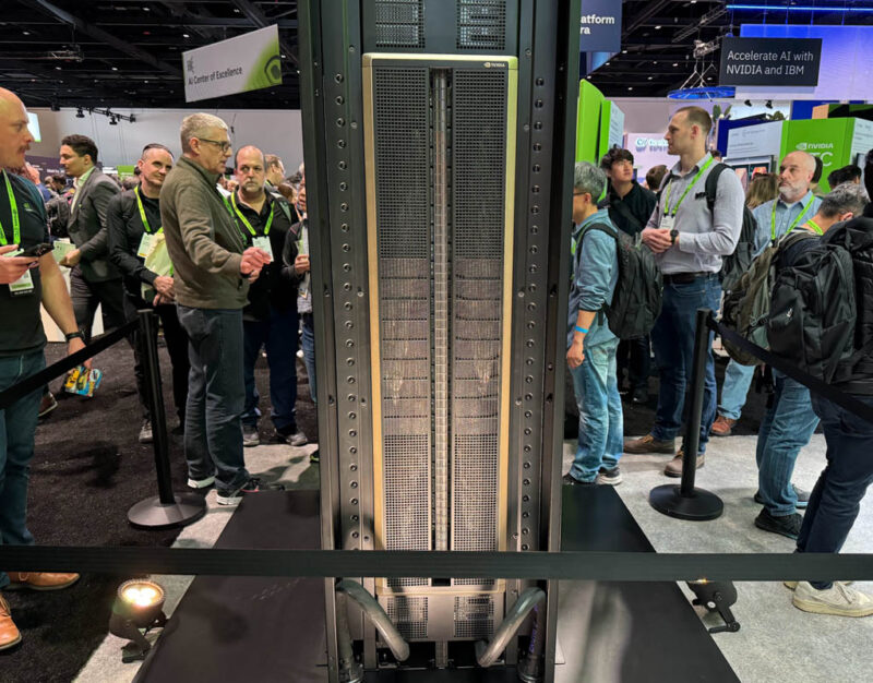
On the show floor at GTC 2024, NVIDIA had a rack configured with its DGX GB200 NVL72. Since we grabbed a few photos of the future of DGX, we thought we would share them. Seeing the physical system makes it feel more tangible.
This is the NVIDIA DGX GB200 NVL72
That may sound like an unwieldy name (I doubled checked that it was the correct name for this system) but it is very descriptive. It is a NVIDIA DGX system. The GB200 tells us we have a Grace Blackwell GB200 compute structure. NVL72 tells us about the NVLink interconnect.
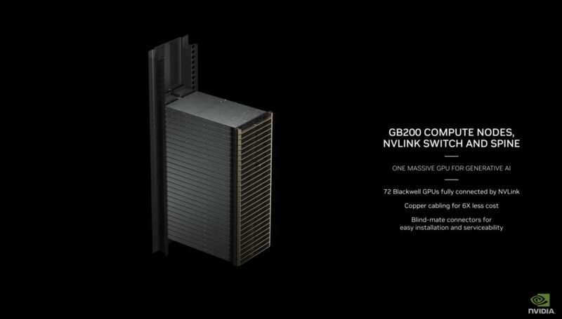
Here is the 120kW flagship system stacked in a single rack. A huge portion of data centers can support a maximum of 60kW racks at this point, so there will be other configurations. We fully expect a half-stack system in the future for those who cannot handle 120kW per rack or nearing 1MW for an 8x rack SuperPOD.
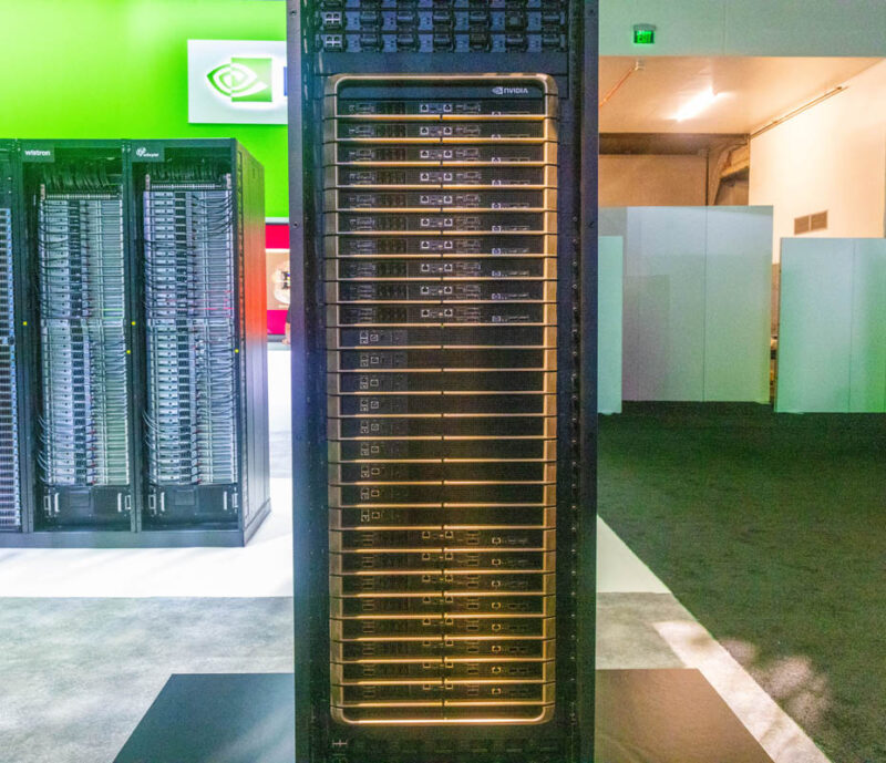
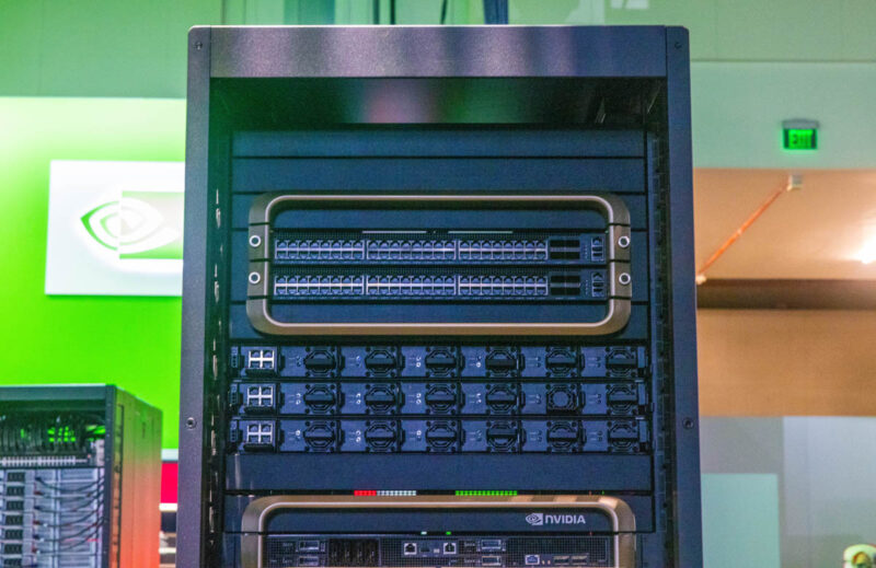
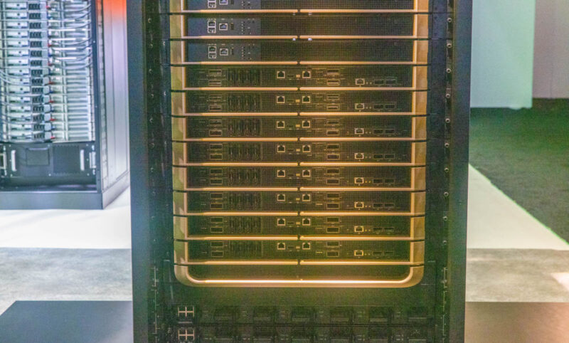
At the top, we have switches.
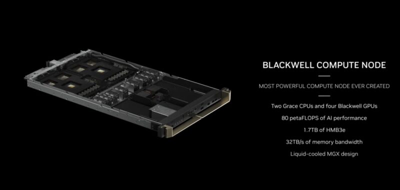
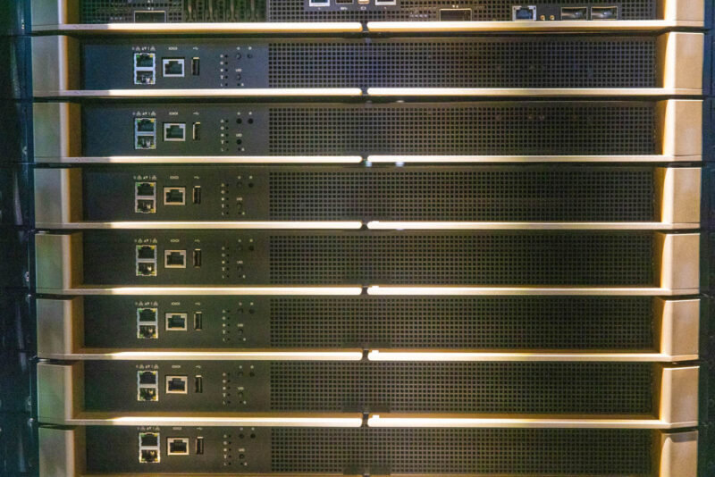
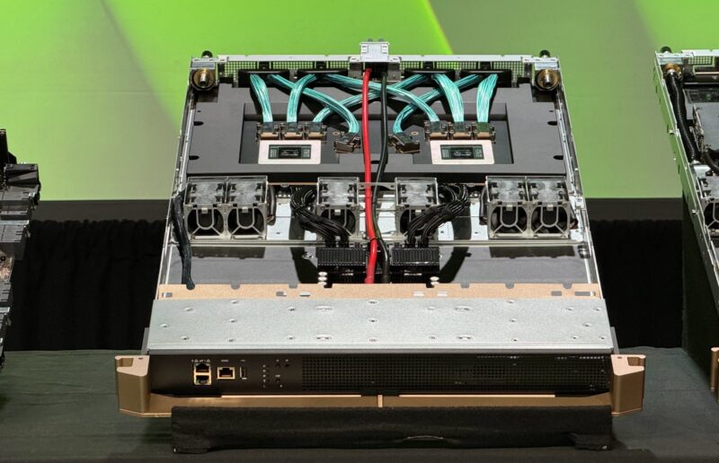
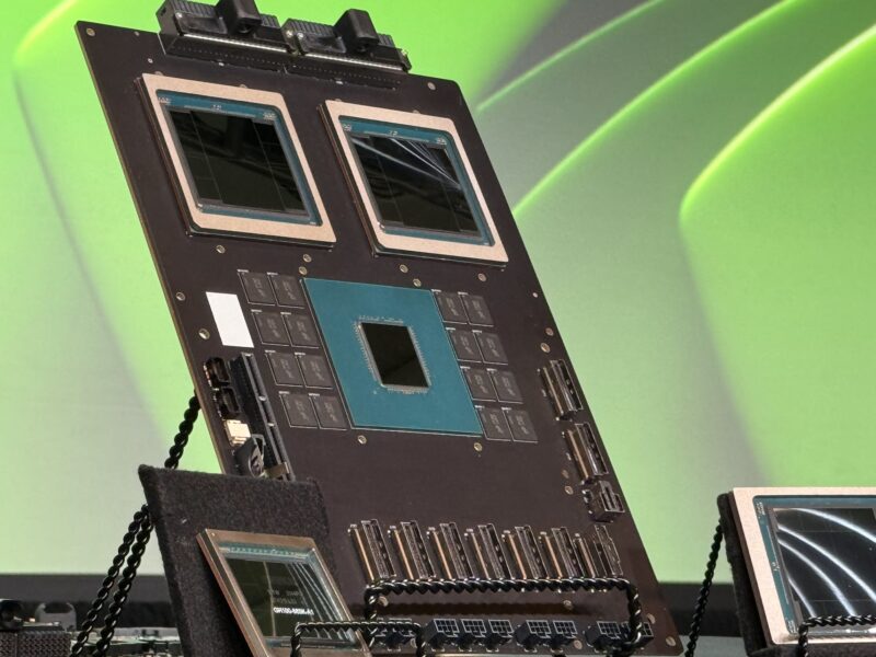
Moving down the stack, we can see the compute nodes. There are ten compute nodes in the top stack. On the front panel we can see each node’s dual Infiniband ports, four E1.S drive trays, and management ports. On the right side we can see the BlueField-3 DPUs.
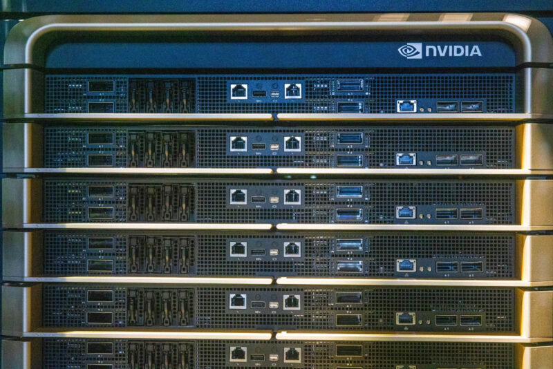
Each of these compute nodes has two Grace Arm CPUs. Each Grace is connected to two Blackwell GPUs for each compute node.
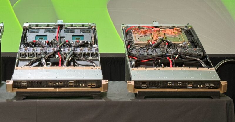
Here is another look at the internals both with and without cooling blocks.
Below these compute nodes are the nine NVSwitch shelves. Something to note is that these gold features are handles to remove the shelves.
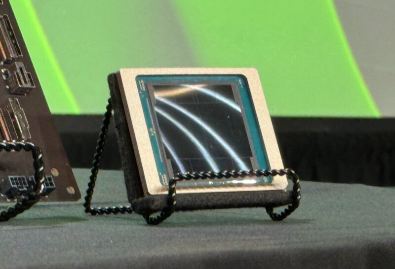
These NVLink Switch trays have two NVLink switch chips.
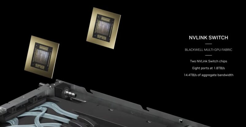
Here is what they look like inside.
On the bottom, we have eight more compute nodes.
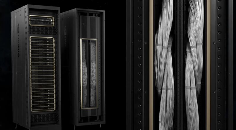
Moving to the rear, we can see that this is a bus bar power delivery design. The rack is designed to blind-mate the power via the bus bar, as well as the liquid cooling nozzles and the NVLink connections for each component. Each needs to allow for a bit of movement to ensure the blind mating works properly.
NVIDIA said that using the copper-cabled NVLink in the rear saves something like 20kW of power in a rack like this.
The net result is one giant system.
Final Words
Hopefully, this was a quick and fun look at the NVIDIA DGX GB200 NVL72. For some who were unsure of what they were seeing, we had our original NVIDIA GTC 2024 Keynote Coverage that goes into many of the components. Still, it is cool to see in person and get a bit of a closer look.
We will have more from the show floor this week, so stay tuned.


So, 120 kW. Are the power bus bars 48VDC, or are they putting AC PSes on each node? In either case, that’s an immense amount of current. 2500A of 48 VDC, or 500A of 240V. Or are they doing something clever here, like really high voltages or high-frequency AC? It’s hard to see how the power losses in conversion would pay off, but sometimes surprising results can pop out of this sort of thing once you factor in cooling, backup power, redundancy, etc.
I mean, trying to run 120 kW through a single copper bus bar at 48V leads to a comically large bus bar. Something like 5 square inches. Presumably they break the bus bar up into segments, and likely have 2 busses as well, but there’s no way to keep that from being enormous. 240V AC is less bad, but still huge.
I just got closer to open systems, so I added a few more photos.
@Scott Laird, looking at the close-up of the system node, you can see two fairly large power cables going into a power board right in front of the fans. It appears to be just a DC-DC converter, so I’m guessing that it’s a single bus running 480 VDC, which would be relatively efficient to get to from 480 VAC 3 phase Wye configuration. By your calculations, that would then be only 250A on the bus, which isn’t terrible.
Holy crap. That’s one hell of a mainframe, if I do say so myself. But why? Why does AI require that much power? Just insane.
@Guy Fisher
My conclusion is 48V. There are 2 sets of 3 power shelves above and below the main compute block. Each shelf has 6 front-ends. This configuration matches with OpenRack V3. The front ends can each be 3KW or apparently soon up to 5.5KW, giving either 108KW or >198 KW of PSU. With the larger ones that is enough for some redundancy even with say 4KW front-ends. Also the compute sleds seem narrower than the power shelves, which would match with an OpenRack design using 21″ widths, but keeping flexibility on the compute side. 48V would be 2500 amps, but fed top and bottom, so no more than 1250 on the bus bar in any location, and only for a short distance.
I have a question about the NVLink networking.
Now my understanding is that each node has 2 boards effectively (in this case a board consists of 2 GPUs and a CPU), like a SuperMicro Twin server.
And then each board has 2 NVLinks of 1.8TB/s per port. Which means 4 ports per node in total.
And then there are 9 NVLink switches that support 8 ports in total per switch. So each 1U NVLink switch can connect 2 nodes.
But how are those 9 switches get connected to each other ? Cause the way it’s presented is like only 2-node sets are connected to each other, for 9 such sets, but no hub connection (or top-of-rack if you will) between the 9 NVLink switches.
For clarity, I’m not talking about the Infiniband or Ethernet connections. In a picture from their presentation it shows that each node has 4 NICs with 2 ports per NIC, at 800Gbps per port. But that is for the inter-server connections, not the GPUs, which in my understanding communicate over NVLink.
@Stephen Beets yes AI power requirements are utterly insane as is the price. These are rough ballparks but a 2000 GPU system will cost ~$80 million to procure, and that doesn’t include the data centre, HVAC etc. The annual electricity bill will be in the region of $8-10 million and you are looking at needing a 3-4MW connection to the electricity grid depending on your cooling method. I spent the first six weeks of this year getting actual quotes from vendors as part of a bidding process to host such a system.
@Panos Grigoriadis
NVLink works in a Peer-to-Peer fashion. Each of the 9 NVLink switch boards has two chips, each providing 4 ports with 18 links, so 9*2*4*18=1296 total.
Each B200 GPU has 18 links. The entire rack has up to 72 GPUs, each with 18 links, which also gives 1296 links total. Thus every GPU can talk to every other GPU in the system.
What I’m wondering is what NVIDIA meant by “fifth-generation NVLink, which connects up to 576 GPUs in a single NVLink domain with over 1 PB/s total bandwidth”. I don’t know how that can be achieved with what was shown for the single rack NVLink networking. That would indeed require something akin to top of the rack NVLink switch. Unless they are using the 800GBit/s “classical” networking in some fashion to connect the 8 racks.
Looking at what was used for Hopper generation it seems that Blackwell NVLink switches shown here are not the only design. Most likely there’s an extended version that contains uplinks to an aggregate NVLink Network Switch. There’s a lot of free space in the chassis.
Hopper used 400GBit/s PHY as base, so it’s not unreasonable to expect 800GBit/s for Blackwell. The Hopper design had a presentation at HotChips 2022.
Thanks Patrick! This is why I come here. Real systems.
BTW, can you confirm the gold handles are 24k or are they merely 18k?
@hoohoo, I think these are oil paint while not real Au Gold.
Comments are closed.