

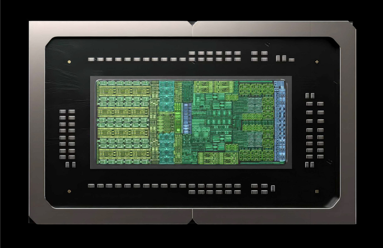
Yesterday we got to look at our first device based on NVIDIA’s RTX Spark SoC: Microsoft’s Surface Laptop Ultra. The latter, the most premium Surface Laptop yet, is the tip of the spear in a broader push within the Windows ecosystem to increase adoption of Arm-based processors. This week NVIDIA is the pole driving that spear tip, with the launch of the RTX Spark.
The RTX Spark launch has been something of a long time coming for NVIDIA. I do not just mean that philosophically. NVIDIA has shipped the underlying GB10 SoC in Linux systems for around a year now, and if the rumors are to be believed, it intended to ship it even sooner. So NVIDIA, its partners, and end-users have been waiting a long time to see what the company’s latest Arm SoC can do when driving a Windows system.

This week, we finally get answers to those questions. Alongside the Surface Laptop Ultra, another half-dozen laptops have been released this week based around the RTX Spark, and there is even a Windows mini-PC (Microsoft’s Surface RTX Spark Dev Box) for good measure. Many of these device manufacturers are taking a similar tack to Microsoft and focusing on developers and content creators, a decision not surprising given what we have seen of GB10 thus far, while others have assembled laptops aimed at the broader consumer market. As a result, although the RTX Spark is a high-end SoC in the vein of, say, AMD’s Ryzen AI Max series (Strix Halo), it is being pitched to a wider user base than we saw with just Microsoft’s laptop.
With that in mind, we wanted to take a moment to briefly run through the RTX Spark, both the chip and the wider platform it defines. What are the similarities and differences between the DGX Spark and RTX Spark platforms? How is NVIDIA promoting its SoC as a new-to-you product for the consumer market? For the answer to that and more, let us dive right in.
NVIDIA RTX Spark N1X Architecture: A GB10 Refresher
First, let us start with the architecture of the RTX Spark. Officially dubbed the “RTX Spark N1X” by NVIDIA, leaving room for future chips in the RTX Spark family, the N1X is the consumer-facing name of our tried-and-true friend in the Linux mini-PC market: the NVIDIA GB10. This is NVIDIA’s latest Arm SoC, and what is really their first SoC in several years that is aimed at end-user systems. GB10 is a high-end design that has seen NVIDIA leverage most of its recent CPU and GPU technologies in a single low-power chip. NVIDIA likens it to a scaled-down version of its Grace Blackwell server architecture, and while it is not an exact scale-down replica, it is not far off the mark, either.
NVIDIA offered a deep dive into the GB10’s architecture back at Hot Chips 2025, and most of what we learned back then still applies to the RTX Spark N1X as well.
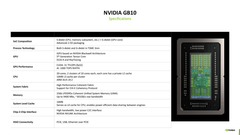
At a high level, GB10 is a joint project between NVIDIA and MediaTek. The chip is comprised of two chiplets. There is a CPU and memory chiplet (the S-dielet) designed by MediaTek, and a GPU chiplet (the G-chiplet) designed by NVIDIA. Notably, both chiplets are built on a TSMC 3nm process, which at the time of GB10’s launch was the most cutting-edge node at the fab and newer than the node used for NVIDIA’s Blackwell-architecture GPUs or its Grace CPU. So, in some respects, GB10 is the most advanced Blackwell architecture chip designed by NVIDIA.
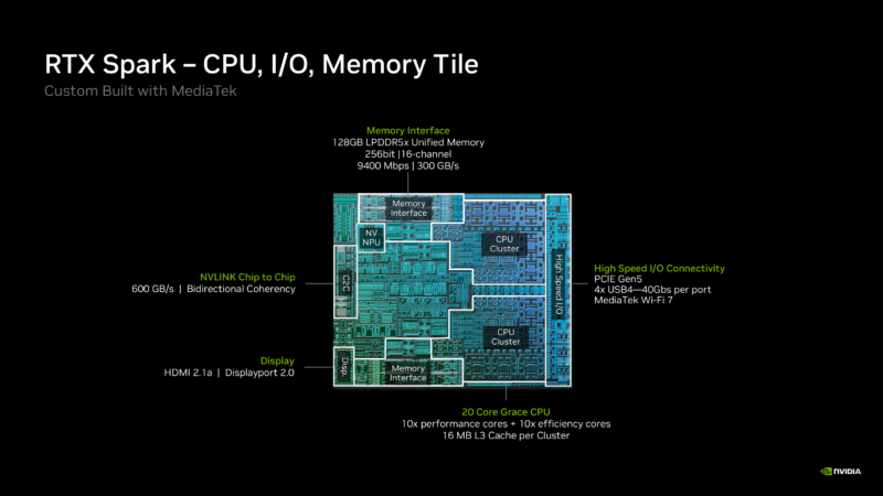
On the CPU die, MediaTek designed a chiplet with four groups of CPU cores, organized into two clusters. The performance cores include a whopping 10 Arm Cortex-X925 cores across the clusters. Meanwhile, the efficiency cores include an equally whopping 10 Arm Cortex-A725 cores across the chip. Each cluster has its own 16MB L3 cache.
This is an off-the-shelf core design from Arm’s 2024 Cortex lineup (not based on NVIDIA’s Grace), so while MediaTek has its own layout, there are no architectural differences from Arm’s stock designs. That NVIDIA is launching a chip based on 2024 CPU cores in 2026 means the RTX Spark N1X enters the market a bit behind the curve in CPU technology, with performance repercussions. In practice, GB10 emphasizes multi-threaded performance over single-threaded performance, especially since this design does not push high CPU clock speeds.
MediaTek’s die also includes the system’s memory controller, which is a key element of its performance. MediaTek equipped the chip with a wide 16-channel, 256-bit LPDDR5X memory bus, making it one of just a handful of (non-Apple) consumer chips to use such a wide memory bus. The wide memory bus not only lets the chip tap into 300GB/second of memory bandwidth (using LPDDRX-9400), but also lets it connect to up to 128GB of memory in its current configuration.
One benefit of NVIDIA’s RTX Spark technology briefings is that they have provided the cleanest GB10 floorplan to date, which lets us see how much space the memory controllers take up. It is a lot of space, though less than you might think given everything else going on.
Surprisingly, the CPU die also holds the chip’s NVIDIA-designed display controllers, even though the GPU hardware itself sits on the other die. This is because display controllers are best placed close to memory controllers for bandwidth and power reasons, and here they sit directly next to one of the memory controller blocks. This is also where all of the general-purpose I/O is located, most notably the chip’s PCIe lanes.
Finally, the chip implements one final piece of NVIDIA IP with its NVLink-C2C interface. The chip-to-chip interface links the two chiplets in GB10, similar to how it connects Grace CPUs to Blackwell GPUs in server-grade GB200/GB300 systems. For GB10, this is a 600GB/second link, making it roughly twice as fast as the memory controllers.
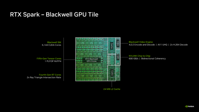
Meanwhile, the other half of GB10 is the NVIDIA-designed G-chiplet. This is dedicated entirely to graphics, and houses a relatively powerful implementation of NVIDIA’s Blackwell GPU architecture. Specifically, this is a 48 SM Blackwell configuration, affording 6144 CUDA cores overall. In the context of NVIDIA’s other offerings, this is equivalent to NVIDIA’s GeForce RTX 5070 in terms of hardware, though the latter has the benefit of over twice as much memory bandwidth thanks to its use of GDDR7.
To be clear, this is a full Blackwell graphics implementation. This is not just a scaled-down version of NVIDIA’s server designs. That is, it has a full suite of graphics features alongside its CUDA cores and tensor cores, including ray tracing hardware, texture units, ROPs, and everything else needed to draw a pixel. This means that GB10 has the hardware needed to support NVIDIA’s full suite of graphics features (DLSS, etc.), which they expect to be a big differentiator in the consumer space.
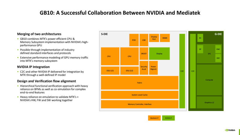
NVIDIA has previously hailed GB10/N1X as being a successful collaboration between the two companies. Whether we will see something like this again in the future is still up in the air, but the fact that this is not a monolithic chip designed solely by NVIDIA is quite notable, given their last 15 years of designing their own Arm SoCs for Tegra, DRIVE, Jetson, and other NVIDIA offerings.




After long time being block for access to x86 share, Nvidia back to x86 realms…. Ehm sorry…. Windows realms for precision.
Ironically just to save Windows in the world of AI development ecosystem.