
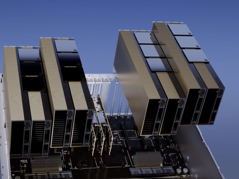
The NVIDIA H100 HVL may look like something we have seen before, but there is a big difference. We asked NVIDIA, and the company says that logically this is two GPUs to the OS, but that the NVLink will allow the full 188GB of memory to be used by the system.
NVIDIA H100 NVL for High-End AI Inference Launched
The new NVIDIA H100 NVL brings two NVIDIA H100 PCIe together with NVLink, and a twist. The new NVL version has 94GB of HBM3 memory per GPU for a total of 188GB. That likely means that the sixth 16GB stack is activated, but with only 14GB available for 94GB of the 96GB active.
What is really interesting as well is the TDP. These are 350W to 400W TDP PCIe cards. Generally, 300W is the top-end we see from most other vendors in PCIe cards since many servers cannot handle 400W in PCIe form factors. That is a big driver for higher-end OAM/ SXM form factors.
| H100 SXM | H100 PCIe | H100 NVL | |
|---|---|---|---|
| FP64 | 34 teraFLOPS | 26 teraFLOPS | 68 teraFLOPs |
| FP64 Tensor Core | 67 teraFLOPS | 51 teraFLOPS | 134 teraFLOPs |
| FP32 | 67 teraFLOPS | 51 teraFLOPS | 134 teraFLOPs |
| TF32 Tensor Core | 989 teraFLOPS1 | 756teraFLOPS1 | 1,979 teraFLOPs1 |
| BFLOAT16 Tensor Core | 1,979 teraFLOPS1 | 1,513 teraFLOPS1 | 3,958 teraFLOPs1 |
| FP16 Tensor Core | 1,979 teraFLOPS1 | 1,513 teraFLOPS1 | 3,958 teraFLOPs1 |
| FP8 Tensor Core | 3,958 teraFLOPS1 | 3,026 teraFLOPS1 | 7,916 teraFLOPs1 |
| INT8 Tensor Core | 3,958 TOPS1 | 3,026 TOPS1 | 7,916 TOPS1 |
| GPU memory | 80GB | 80GB | 188GB |
| GPU memory bandwidth | 3.35TB/s | 2TB/s | 7.8TB/s |
| Decoders | 7 NVDEC 7 JPEG |
7 NVDEC 7 JPEG |
14 NVDEC 14 JPEG |
| Max thermal design power (TDP) | Up to 700W (configurable) | 300-350W (configurable) | 2x 350-400W (configurable) |
| Multi-Instance GPUs | Up to 7 MIGS @ 10GB each | Up to 14 MIGS @ 12GB each |
|
| Form factor | SXM | PCIe Dual-slot air-cooled |
2x PCIe Dual-slot air-cooled |
| Interconnect | NVLink: 900GB/s PCIe Gen5: 128GB/s |
NVLink: 600GB/s PCIe Gen5: 128GB/s |
NVLink: 600GB/s PCIe Gen5: 128GB/s |
Based on the specs, it seems like, assuming the NVIDIA H100 NVL specs are for 400W, that the PCIe versions are vastly superior to the H100 SXM5 versions but without the higher-end 900GB/s NVLINK interfaces. The compute specs are 2x the H100 SXM, but the NVL version has more memory, higher memory bandwidth, and uses similar power for the performance.
Final Words
Our sense is that the NVL will have to be de-rated or the H100 SXM5 will need a spec bump soon to match. This is very strange positioning. Still, NVIDIA says that OpenAI that is using DGX A100’s now for ChatGPT can replace up to 10x DGX A100 systems with four sets of NVIDIA H100 NVL pairs to do its inferencing. It will be interesting to see whether these get de-rated or an updated H100 SXM5 over time.


“Based on the specs, it seems like, assuming the NVIDIA H100 NVL specs are for 400W, that the PCIe versions are vastly superior to the H100 SXM5 versions given they are 300W less but without the higher-end 900GB/s NVLINK interfaces.”
TDP is a design specification. Just because the SXM part can be configured to allow it to operate at 700 W doesn’t mean it needs 700 W to operate. A processor can be limited by various different things for its performance, power being just one of them. Just because a processor can draw 700 W doesn’t mean it needs to in order to perform a certain workload as fast as one that can only draw 400 W. The SXM form factor may allow for a much better cooling solution than the PCIE card. That would allow increased performance for workloads that are power-limited.
“The compute specs are 2x the H100 SXM, but the NVL version has more memory, higher memory bandwidth, and uses 57% the power for the same performance.”
I think there is an error in your reporting here. The specs quoted here are for the two cards **together**. As such the H100 SXM still enjoys a clear positioning in the market if you ask me.
Good point folks. Let me fix that.
Just checked with Dell, they have them in new XE9680, but seams that lead time is a bit high…
Seems like a vram bump, and one has to buy in pairs to get it. Which is just more market segmentation in my books.
If, as the marketing vaguely implies it was transparent shared address space btwn the two GPU chips that’d be cool. But it actually looks like a pair of H100 connected by, OMG!, nvlink.
Comments are closed.