
At Hot Chips 32 (2020) Intel gave additional detail around their Tofino2 (previously this was “Tofino 2”) programmable switch chip. This comes just over a year after Intel acquired Barefoot Networks for Ethernet Switch Silicon. Barefoot does not make just a fixed-function switch chip. Instead, it uses a programmable architecture which makes it in many ways more interesting. The Tofino2 generation is where we expect to see co-packaged optics using silicon photonics. We already had the chance to see this working in Intel’s lab.
Video Resource
If you want to learn more about the Intel Tofino2 co-packaged optics that we are going to discuss in this Hot Chips 32 presentation, we did a piece at Intel earlier this year:
The system we have in that video is the same that Intel is showing at HC32.
Intel Tofino Background
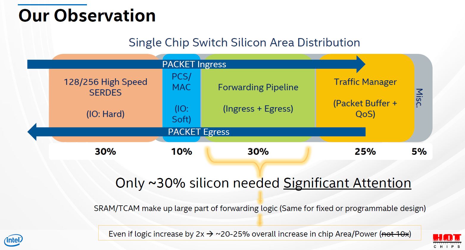
The Barefoot team, and presumably the Intel team before acquiring Barefoot, realized that there was an opportunity to add programmability into switch chips instead of having them be a fixed-function device. Intel is highlighting that there is a lot of silicon dedicated to some of the basics, but additional functionality can be added at a relatively minimal silicon cost for where one would want logic. As an example, a SerDes is going to be fairly hardened logic while the pipeline may benefit from having programmable logic.
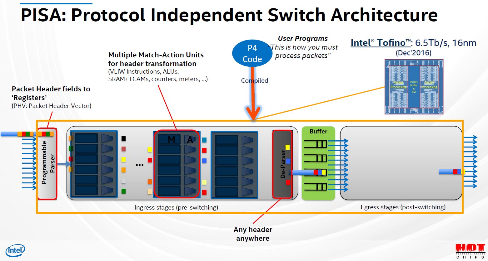
The Barefoot, now Intel Tofino chip utilized P4 code for programming the switch to look for packets and provide processing rules.
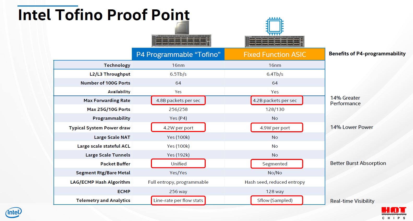
Intel uses 6.5Tbps for Tofino but most of the industry would call this a 6.4Tbps class switch. Here Intel found that it actually got better performance and lower per-port power using the programmable architecture. There are other features such as telemetry data and some features that could be added via the new architecture as well. For anyone that wonders, the industry usually uses Broadcom Tomahawk and Trident lines as their standard comparison points.
Next, we are going to look at how those impact Tofino2.
Intel Tofino2 Next-Gen Programmable Switch
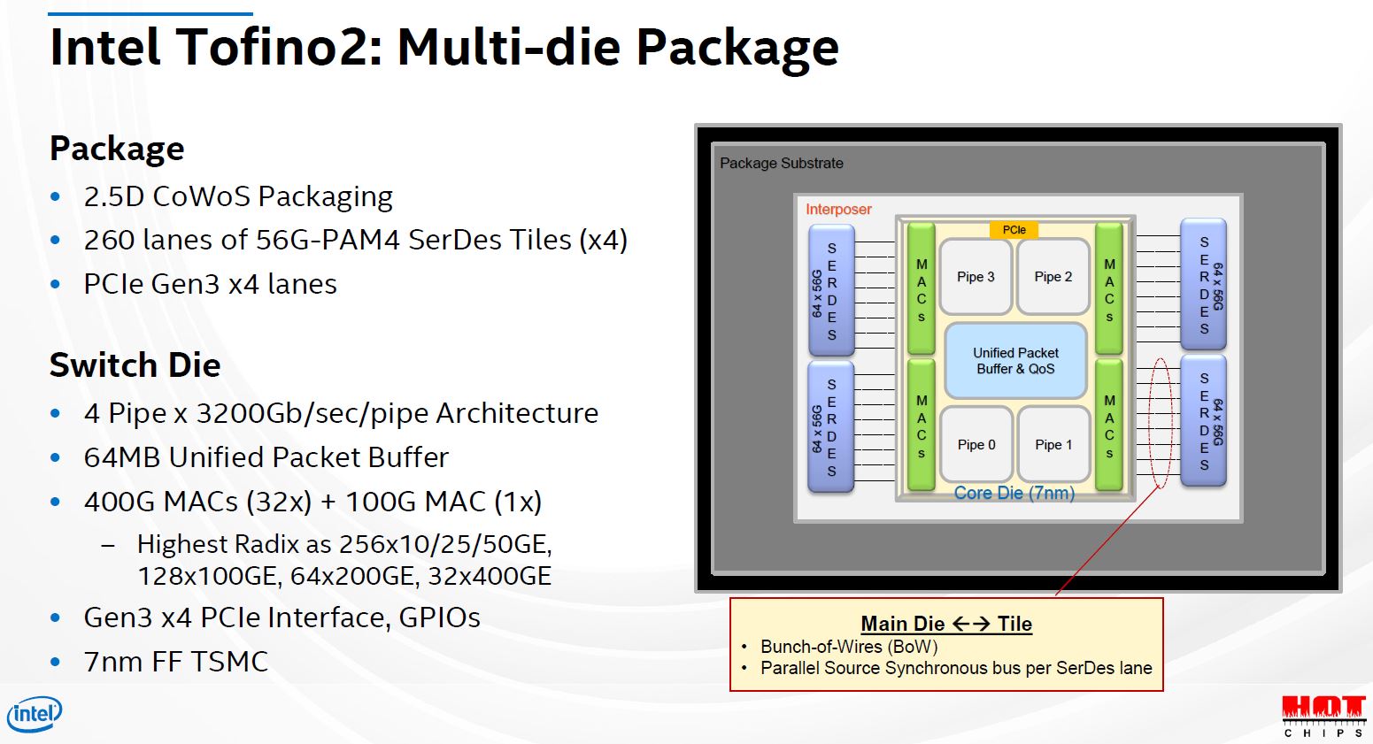
Given that proof point, Intel is using a multi-chip die for its 12.9Tbps (12.8Tbps) generation switch.
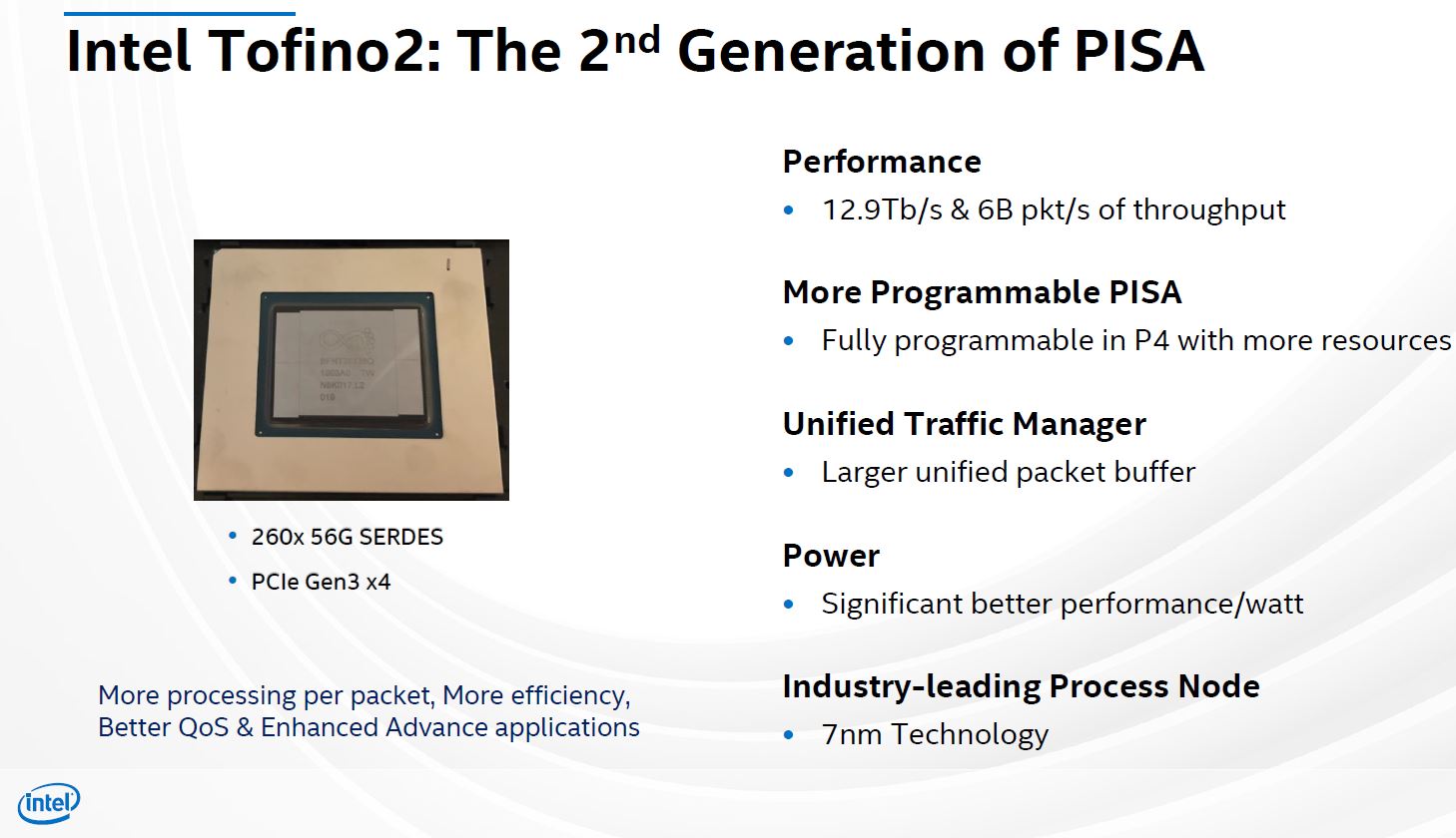
This is being built on TSMC 7nm and utilizes CoWoS packaging as we would commonly see in GPUs. Of note, during the Innovium TERALYNX 8 25.6Tbps Switch Chip Launch we asked why they have a monolithic die, and the company said they did not need to disaggregate SerDes yet.
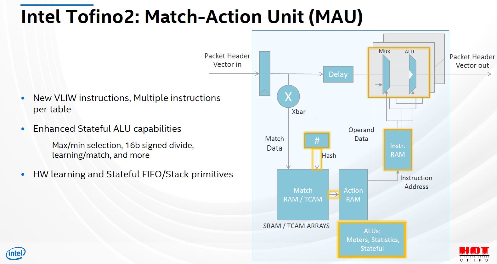
A big part of the Tofino2 value proposition is being able to analyze packets and decide what to do with them at very high speeds. That is a key function of the Match-Action Unit or MAU.
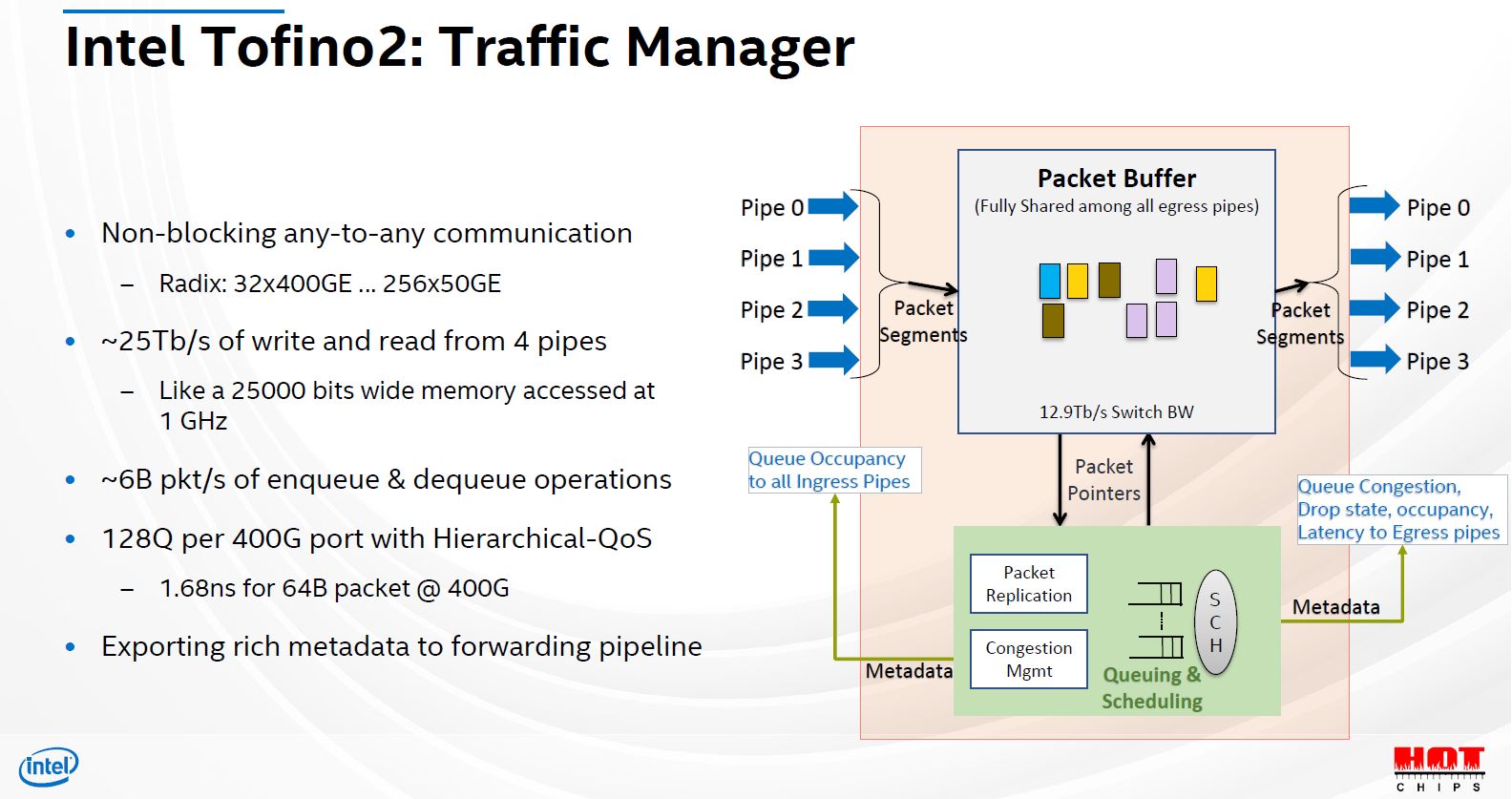
With so many packets moving through the switch silicon, the Traffic Manager is going to be an area of focus. Intel is focusing on a 6B packet/ second switch chip with many of the QoS features we would expect on this generation of switch.
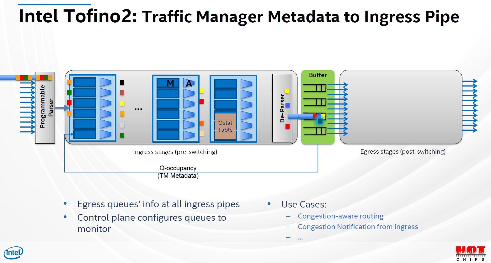
Intel discussed how the new Tofino2 Traffic Manager can service use cases such as congestion aware routing.
One of the other big features with Tofino2 is co-packaged optics.
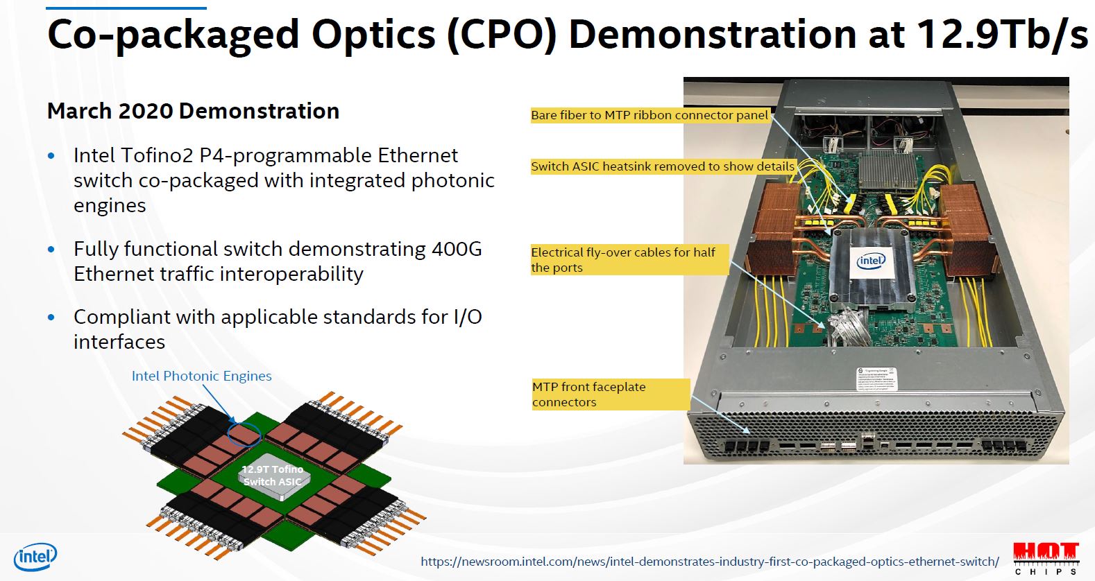
See our piece Hands-on with the Intel Co-Packaged Optics and Silicon Photonics Switch for more detail on this demo including seeing the setup pass 400Gbps traffic. Other switch vendors are thinking it will be another generation or two until this is needed. Intel is a bit earlier. That is likely because Intel also has the silicon photonics IP and is shipping it to big customers such as Facebook already.
Final Words
Programmable switches are a hot area of focus these days. In Intel’s HC32 presentation, the company was talking about AI work enabled by data plane programmability. While that may or may not be the killer next-gen use case, the solution provides something simple: it is a building block. Customers can deploy switches and instead of waiting for new hardware to add functionality to address the “what if we could…” question, programmable switches make that a software question.


IDK Patrick, for the hyperscalers and public cloud operators modifying how Ethernet frames are parsed may be useful. For the rest of the world it seems to be overkill.
Perhaps Intel is going to make another foray into Infiniband or similar?
Of course this is for large providers. High performance networking staff is very expensive, but intel will save huge amount of space in datacenters by replacing multiunit switches.
Fuck intel
Fuck mani ramkumar
Comments are closed.