

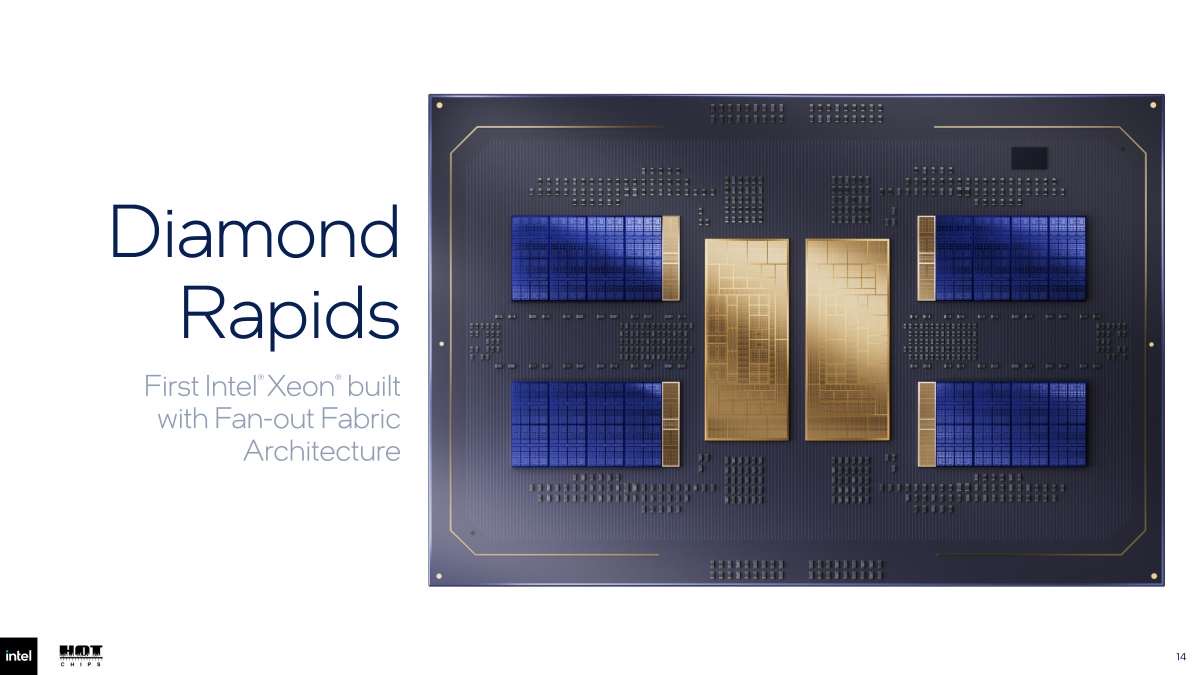
Intel is presenting Diamond Rapids, its next-generation Xeon server platform, on day one of Hot Chips 2026. It is the follow-on to Xeon 6 “Granite Rapids” and a central piece of Intel’s data center roadmap, with the Xeon 7 “Diamond Rapids” platform now slated for 2027 after Intel shifted its timing earlier this year. Also, it sounds like the 256-core was just added to the roadmap very recently. To be fair, Intel is selling just about everything it makes these days, but the next-generation Coral Rapids is an enormous family, and I cannot wait to see that one, hopefully at next year’s Hot Chips 2027.
We are writing this one live, so please excuse any typos as the presentation moves quickly.
Intel Diamond Rapids at Hot Chips 2026
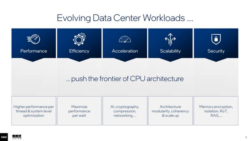
Intel opened its talk by setting four pillars for the platform: performance efficiency, acceleration, scalability, and security.
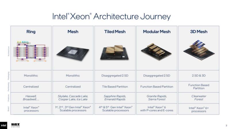
Intel walked through the mesh lineage that leads to Diamond Rapids. It runs from monolithic ring and mesh designs, through the disaggregated 2.5D tile partitions of Sapphire Rapids and Granite Rapids, to the 2.5D and 3D function partitions of the current generation, which puts Diamond Rapids at the top of Intel’s modular trajectory.
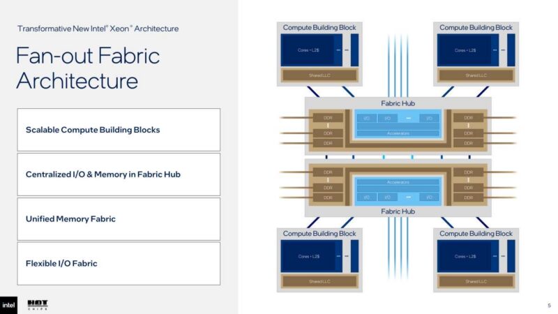
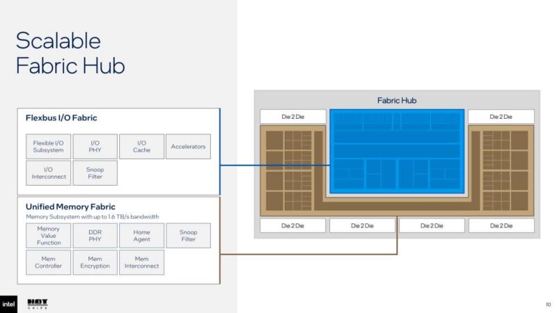
At the heart of Diamond Rapids sits a set of scalable compute building blocks built around a Fabric Hub. Each Fabric Hub centralizes memory and I/O, and the compute building blocks connect through a unified memory fabric plus a flexible I/O fabric. The idea is that each compute building block chiplet connects directly to the fabric hub, and you can scale the fabric hub. This is really neat stuff.
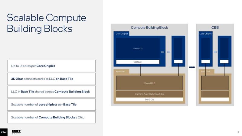
Inside a compute building block, core chiplets each hold up to 16 cores and connect to a last-level cache on a base tile via a 3D crossbar. That last-level cache is shared across the whole compute building block, and Intel scales both the number of core chiplets per base tile and the number of compute building blocks per chip.
Intel calls the connection side the Flexbus I/O fabric, with a unified memory fabric feeding a memory subsystem designed for up to 1.6 TB/s of bandwidth. Snoop filtering and home agents sit on die so coherence stays local to the fabric rather than spanning the whole platform.
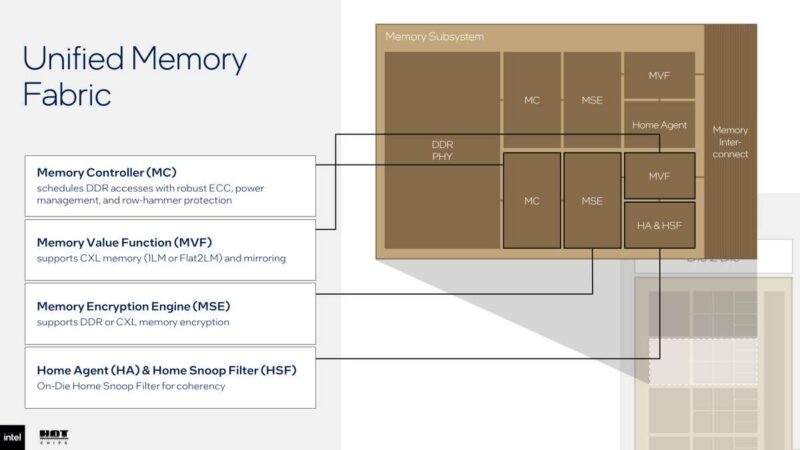
Memory lands in the Fabric Hub through a controller that schedules DDR with robust ECC, power management, and row-hammer protection. A memory value function brings in CXL memory in one-level or flat two-level mode with mirroring, and a memory encryption engine covers both the DDR and CXL paths.
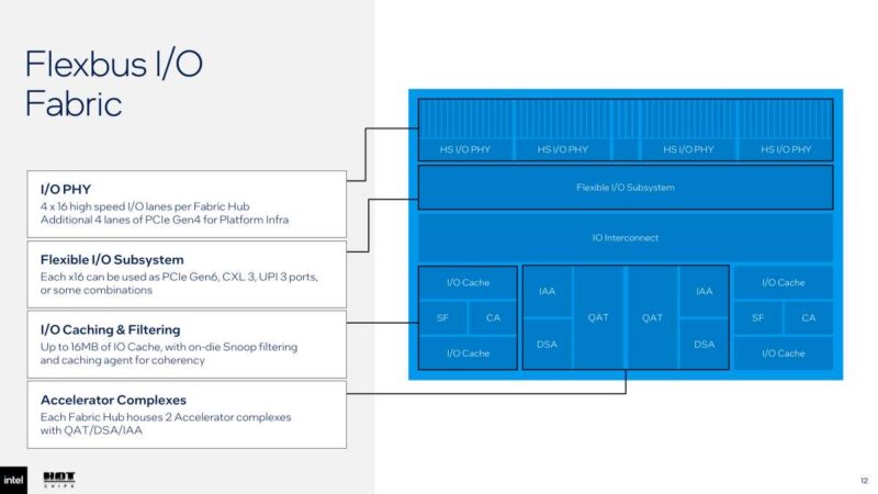
This flexible I/O subsystem provides four x16 ports on each Fabric Hub, and each x16 port can be configured as PCIe Gen6, CXL 3, or UPI 3. Each Fabric Hub also carries up to 16 MB of I/O cache with on-die snoop filtering and two accelerator complexes housing QAT, DSA, and IAA.
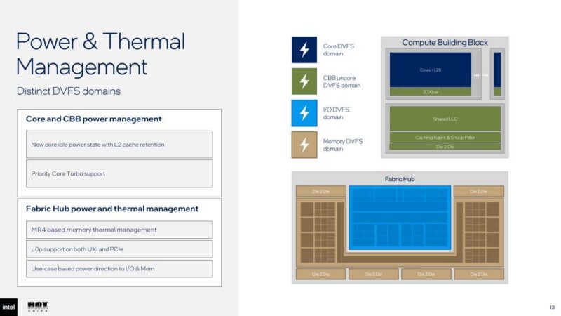
Power management is designed at the compute building-block level. Intel described a new core idle state with L2 cache retention, priority-core turbo support, MR4-based memory thermal management, and low-power L0p support over both UXI and PCIe links.
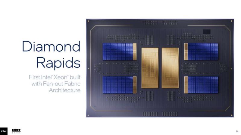
Diamond Rapids ties these pieces together as the product itself, and this figure frames the platform that Intel is presenting across the session. Just as a note here, this looks a lot more AMD EPYC style (albeit with clear differences) than it does NVIDIA Vera, Arm AGI CPU, and others.
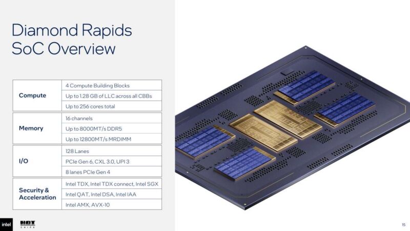
A flagship configuration combines four compute building blocks for up to 256 cores and 1.28 GB of last-level cache. Sixteen memory channels feed the platform with up to 8000 MT/s DDR5 and up to 12800 MT/s MRDIMM, and I/O spans 128 lanes of PCIe Gen6, CXL 3.0, and UPI 3 plus 8 lanes of PCIe Gen4. Those memory speeds build on the Gen 2 MRDIMM and DDR5-8000 modules STH saw on display recently.
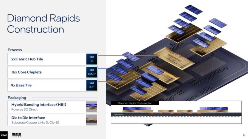
At the package level, Diamond Rapids stacks two Fabric Hub tiles, 16 core chiplets, and four base tiles. Core chiplets connect to the base tile through a hybrid bonding interface using Foveros 3D direct die-to-die, while substrate copper links carry the interconnects out to the Fabric Hub tiles.
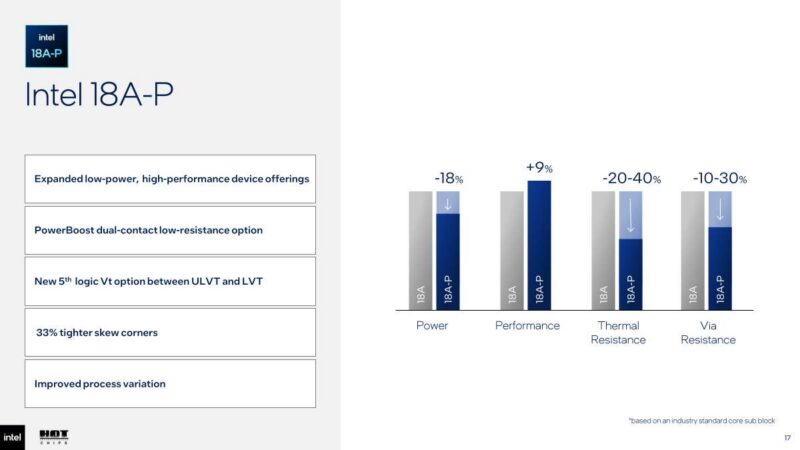
Built with Intel’s 18A-P process node, the platform draws on an expanded set of low-power and high-performance devices. That includes a dual-contact PowerBoost option, a new logic threshold option between ULVT and LVT, and 33 percent tighter skew corners.
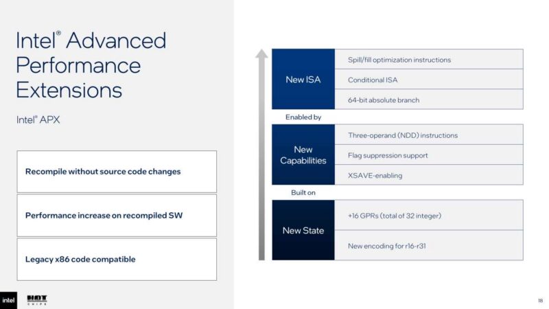
Intel is adding what it calls spill-and-fill optimization instructions to the ISA. That set adds 16 general-purpose registers for a total of 32 integer registers, introduces new encodings for registers r16 through r31, and adds three-operand instructions while remaining compatible with existing x86 software that recompiles without source changes.
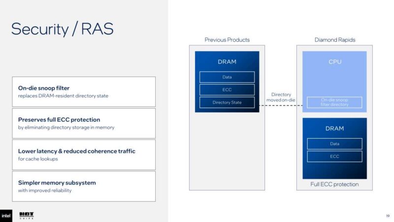
Coherence data also moves on to the die. Intel replaces DRAM-resident directory state with an on-die snoop filter, which preserves full ECC protection by removing directory storage from memory and, in turn, lowers latency and cuts coherence traffic.
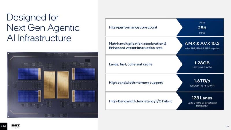
That performance with 256 cores, 1.28 GB of cache, 1.6 TB/s of memory bandwidth, and 128 lanes of high-bandwidth, low-latency I/O. Matrix multiplication acceleration rides on AMX and AVX 10.2 with expanded vector instruction support.
Intel closes the session with the full Diamond Rapids summary. This wrap-up folds the modular compute building blocks, unified memory fabric, 18A-P process technology, and the security and acceleration engines into a single architectural picture.
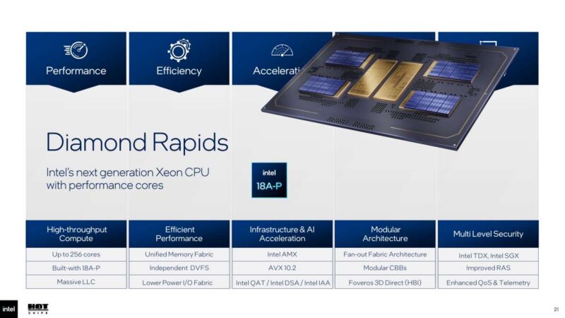
That covers the Diamond Rapids architecture as presented in today’s talk.
Final Words
Diamond Rapids is Intel’s answer to the high-core-count, high-memory-bandwidth server lane as the platform heads toward 2027 against AMD’s EPYC push. It seems like Intel updated its roadmap recently to match AMD’s 256 cores since AMD’s 256-core design is an all-P-core design (albeit with 512 threads). Moving coherency on-die, stacking with 3D, and stepping up to the 18A-P process all help close the efficiency gap with the competition. Still, it seems like Diamond Rapids is going to be a second-half-of-2027 part, so we have some time to go.


Diamond Rapids feels like a weird dual die chip from years past. The two fabric hub dies seems like an afterthought as if the socket was originally designed for one. On the topology side, this maybe a nonissue if each compute block had a link to each fabric die through the substrate. The diagrams point toward the two fabric links connecting to two links the nearest fabric die.
The chiplet topology seems to be a step backward by going to some SerDes over the packaging. Intel’s usage of bridge chips was complex and costly but it really did permit multiple dies feel like one large monolithic beast. The issue Intel had is that they did not create a topology that was flexible nor scaled well. Even now, I don’t see many of the chipsets or interfaces being re-used in the future. Intel is putting a lot of heavy engineering into topology concepts that will last a single generation. Where else is Intel going to use these compute building blocks? Will the base die of the compute building block need to be redesigned for a new generation of CPU cores?
There does seem to be a silver lining in that if Intel went to a single link to the compute building block, they could double core counts to 512. I would presume these links and the fabric does would become congested as that would be a lot of access pressure for data traffic. For workloads that could tolerate this, performance would be impressive.