Today, Intel made a few disclosures about the future of its process technology. At this point, nobody (Intel included) would say that the 14nm to 10nm transition was a runaway success that was on or ahead of schedule. Intel is trying to re-spin its manufacturing story, and part of that includes new node names as well as some process innovations.
Note: We are doing this live after some pre-brief. We will be updating this as the event unfolds.
New Intel Accelerated Manufacturing Node Names
One of the big drivers for re-naming its process is competition. Some may argue it is not, but let us face it, TSMC says it is on 5nm and 7nm while Intel says it is on 10nm for its leading-edge process. That does not look great in a world where smaller has meant better for decades. Indeed, progress has been defined by smaller numbers that loosely at some point related to feature sizes but that is a bit dated of a way to think about process technology.
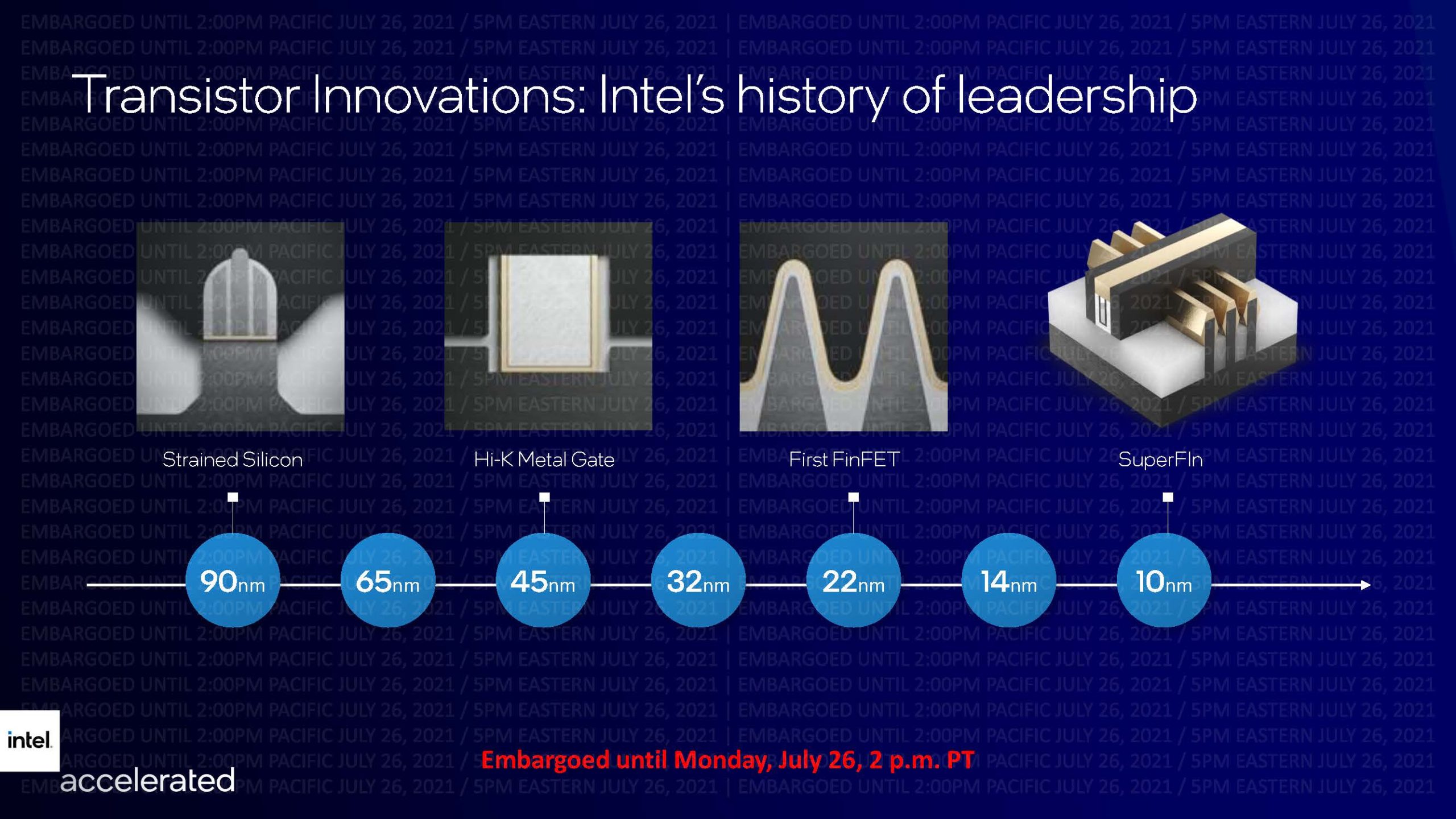
Let us get to the new naming. The 10nm SuperFin solution is going to still be called 10nm, but after that we are losing the “nm” in process terms. Intel is renaming its current 10nm Enhanced SuperFin to Intel 7. We can read into this that the reason is to position it aligned to TSMC 7nm. Intel 4 was previously Intel 7nm. Intel 3 is better again. Intel 20A is going into the angstrom era hence the “A”.
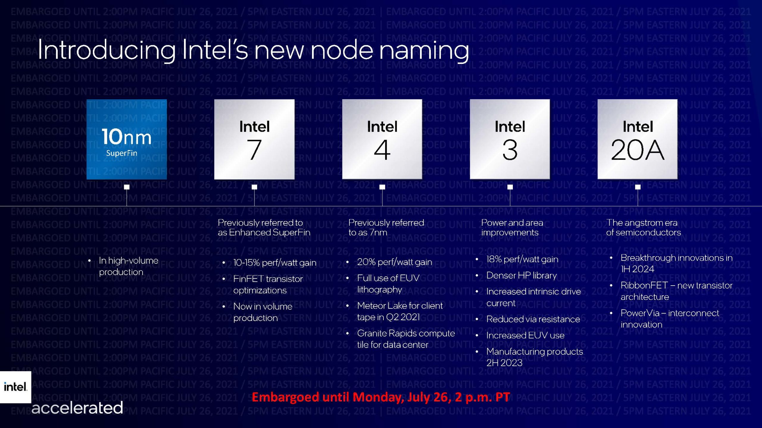
While you can read the text in the chart above, there are a few items we wanted to point out. First, we have the “Granite Rapids compute tile” for a future Xeon. Intel is fully embracing the “glued together” CPU methodology and that is why we have a compute tile in Intel 4. Meteor Lake will also be on Intel 4. Intel 3 is slated for 2023 which likely means volume products in 2024 if that schedule holds since there is typically a lag between manufacturing and availability. Also, 2H 2023 includes a December 31, 2023 start of manufacturing.
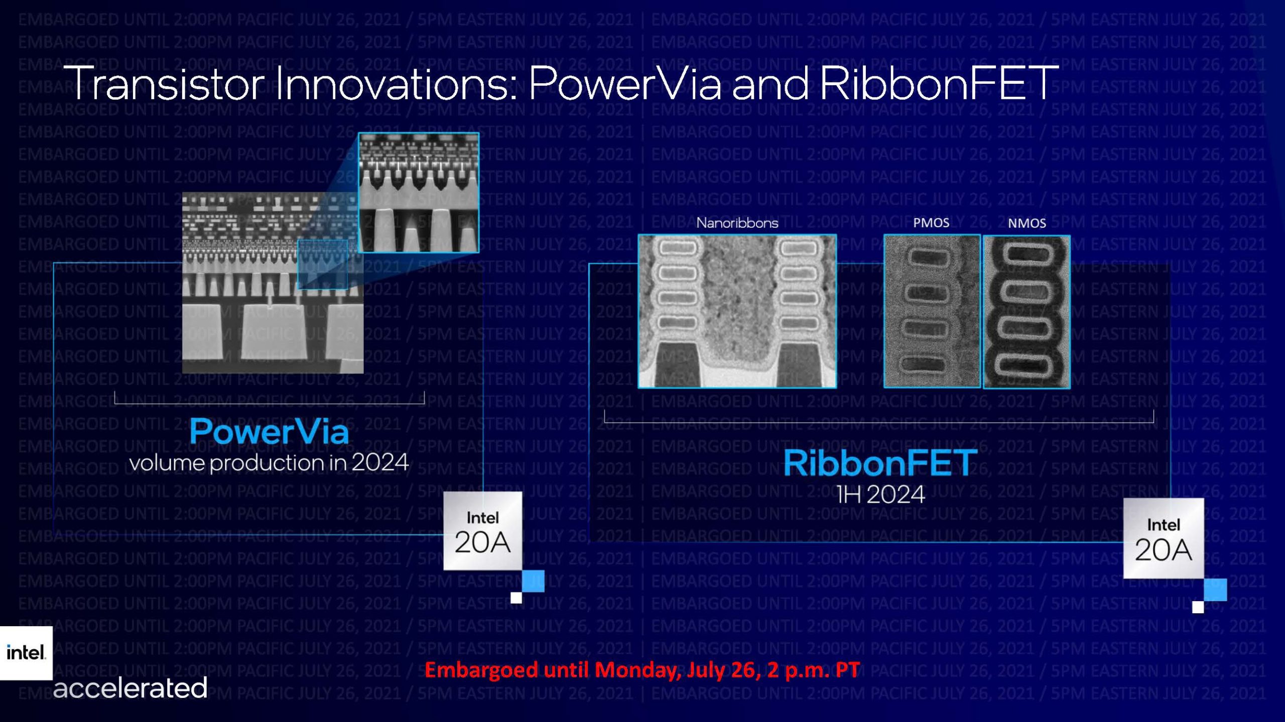
In 2024, Intel will move to Intel 20A. There we get a few new innovations. First is the Intel PowerVia where power is delivered from below by vias thus allowing the top of chips to be used more effectively since power delivery has its own channel. Intel says this will have better resistance/ capacitance while also freeing up more area near the logic gates. On the gates, Intel has a new gate all around technology it is calling the Intel RibbonFET. TSMC is also working on gate all around designs, but this shows where the industry is headed.
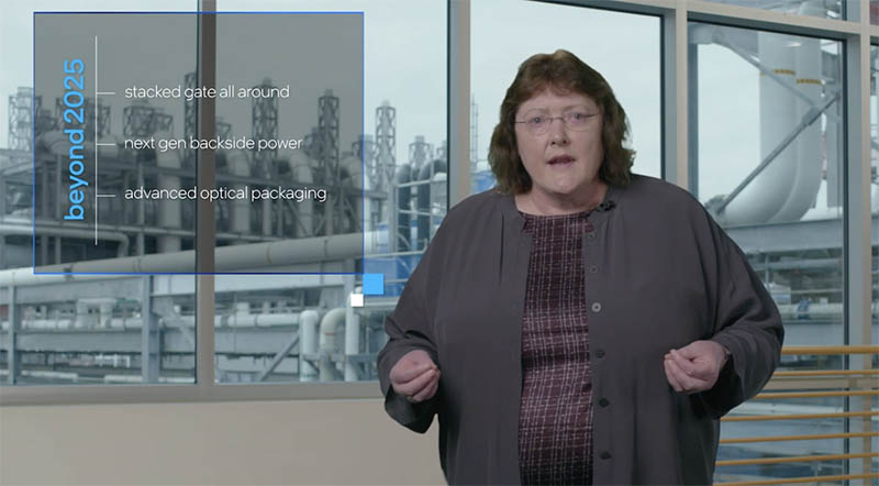
Intel also said that 18A would be 2025 production, but that is still in development. Intel also said that it will look to switch from copper/ electrical to optical in the future.
Beyond the chips themselves, a big part of the story is packaging. We have discussed EMIB and Foveros often on STH. These technologies allow Intel to combine silicon, from heterogeneous processes/ manufacturers, either next to one another in a 2D array or stacked to make 3D chip stacks. Sapphire Rapids Xeons will be the first mainstream product with EMIB. Intel says this is more power-efficient and faster than package interconnects (e.g. AMD EPYC.)
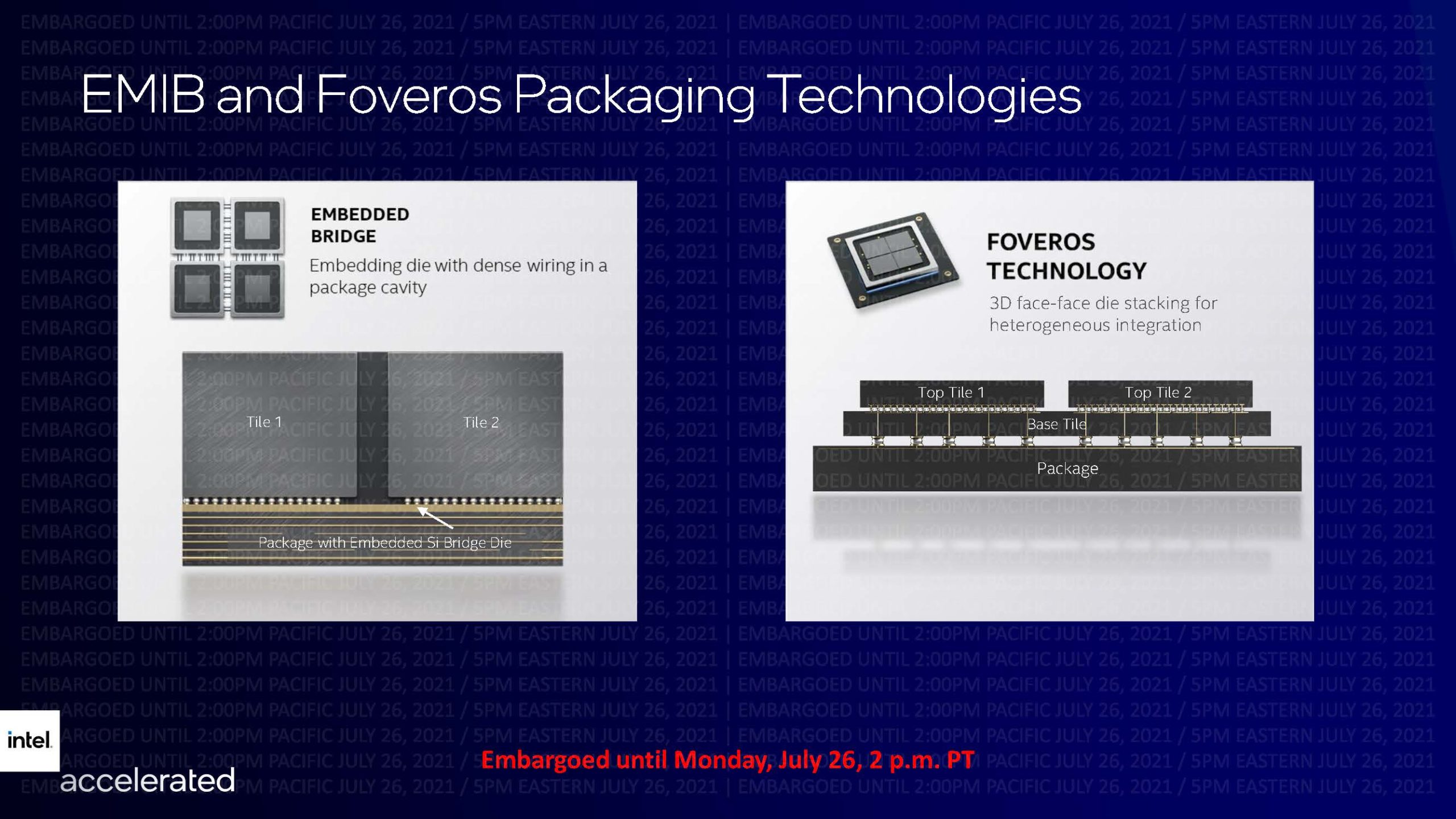
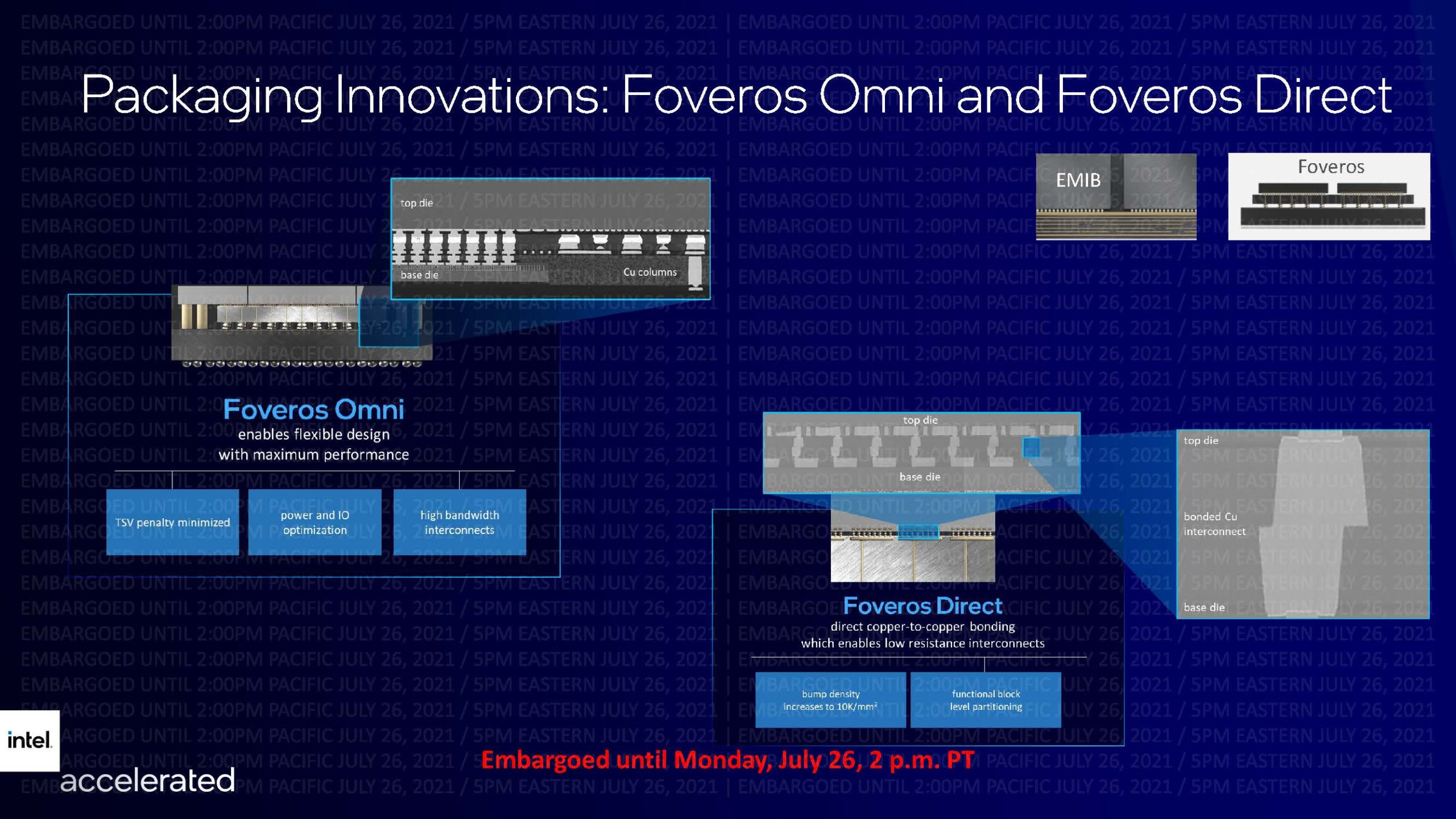
Intel is now discussing its Foveros Omni and Foveros Direct. These allow Intel to stack chips with more performance on the stack. One of the biggest challenges with adding multiple dies to a stack is the number of and type of physical connections between the different pieces of silicon and that is what Intel is addressing here.
While the above is focused on 2021 to 2024, Intel expects to be at a leadership point by 2025.
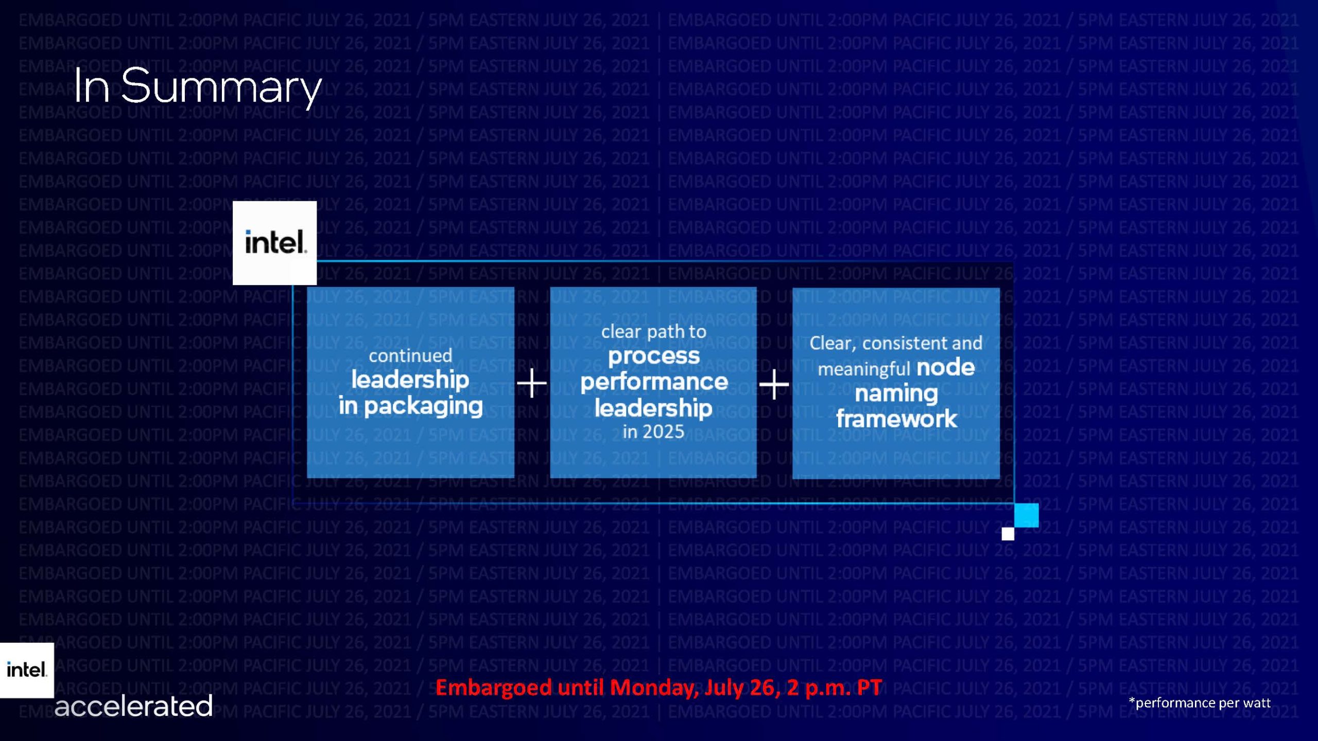
This may seem like a mundane slide, but it is an important one. Saying it will be in a leadership position in ~4 years is an implicit recognition that it is not in a leadership position today. Publicly and directly admitting this is a big step for Intel.
Intel IDM 2.0
One of Intel’s big plays is with IDM 2.0. Intel has its own fabs for its own products as it has done for years. Intel will also use external foundries which it has also done for years. The big change is the new focus on the Intel Foundry model that we covered in Pat Gelsinger Starts to Revamp the Intel Borg.
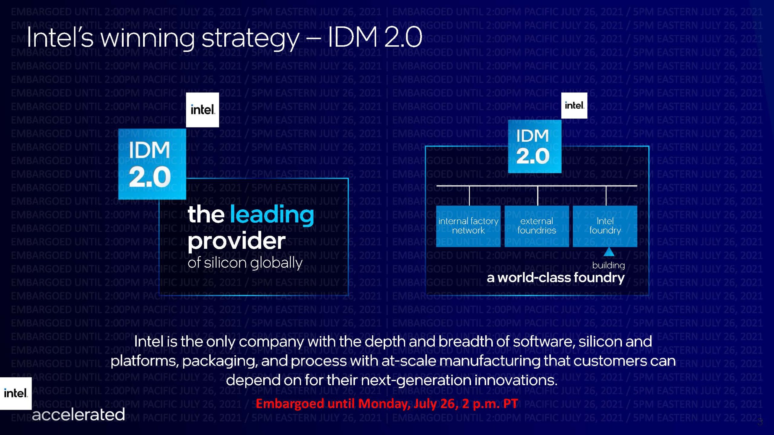
Part of the company’s strategy is to show that it can produce leading-edge products. It is then shopping itself as an alternative to TSMC to governments saying that it can produce chips so that geopolitics do not threaten chip supply.
Final Words
During a pre-brief call, I asked Intel about its product mix on the leading-edge process. With 10nm, as an example, Intel “launched” 10nm well before we saw it in mainstream server and desktop parts. The line of questioning was to gauge if Intel was committing to guidance in terms of not just having leading technology, but also if it can mass-produce chips with that technology. Instead of addressing that, Intel focused on saying that it will meet business units’ needs. This is important because the server group may have needed 10nm Ice Lake but delays in volume manufacturing meant that product was delayed by many quarters.
Perhaps the way to better read today’s announcement is that Intel is positioning itself to US, EU, and other governments saying that it can deliver high-end semiconductors without the geopolitical risk of TSMC. Assuming Intel gets investment, that allows for more R&D money and manufacturing capacity as a way to become a cornerstone in the supply chain even in a heterogeneous manufacturing environment with multi-die chips.


So who is the Buzzword Engineering aimed at?
Major accounts won’t fall for it; they’ll just bench their actual apps and check quotes as always.
Enthusiasts are already snickering, and will focus on such objective general benchmarks as eventually turn up, tempered by price, availability and brand bias.
Investor? Checking in on INTC for the week, they raised an eyebrow, then lowered it.
Won’t address all the issues re IDM 2.0 webinar. Mr. Gelsinger, does INTC still plan to build U.S. and EU foundries if it doesn’t receive subsidies? Mr. Gelsinger, INTC has a very poor “track record” when it comes to external foundries. Why do you think INTC will be successful this time? Yes it is true that INTC has relied on external foundries, and this hasn’t changed. Why is INTC planning to use TSMC for 3nm? Rumored to be in 2022. Ignoring the IDM 2.0, isn’t the main reason INTC is in the mess it is, is because it has lost the lead in “leading edge” process nodes. What makes you think TSMC is going to be doing nothing while you try and catch them in the process nodes? What kind of margins do you expect from these proposed new U.S. and EU foundries? Finally, overtaking TSMC in the process nodes race & IDM 2.0 plans are ambitious objectives. Wouldn’t it be more profitable & less of a financial risk, if INTC focused soley on recovering the process node lead, and forget about bldg. new foundries in the U.S. & EU.?
Comments are closed.