
Building an Entire CPU is Entirely Different
Many think that all you need to do is call Arm, get some cores, and magically a CPU appears. If that was not clear from the previous section on the Arm AGI CPU, building a physical CPU involves much more than selling an Arm Neoverse V3 core IP. You still need to connect those cores together. You need memory controllers, PCIe controllers, and security controllers. Once you have all of the features and have designed it, then you need to get the chip fabricated, in this case at TSMC.

Some of the key areas of the design process:
- Architecture Definition and Design
- Microarchitecture and RTL Design
- Pre-Silicon Verification: Simulation, Emulation, and FPGA
- Physical Design and Tape-Out
Some of the above the Arm Neoverse CSS V3 gets you, but clearly not all of it. Once the chips are fabricated, they then need to be packaged. Then the real fun work at this ATE Lab begins.
- Post-Silicon Bring-Up
- Validation, Characterization, and Binning
- Manufacturing Test and Ecosystem Ramp
That may all seem simple, but it is not. You have to check that every wire from the CPU works as intended and within spec. Then you need to ensure the firmware can deliver a working system. Once that is done, the next step is to ensure the chip and firmware work with your ecosystem of hardware and software partners.
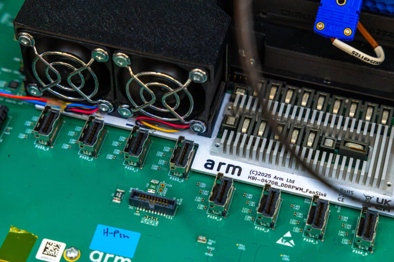
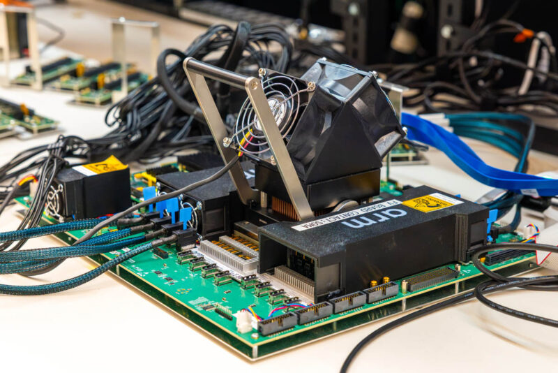
A key part of this is the Arm Functional Validation board for the AGI CPU.
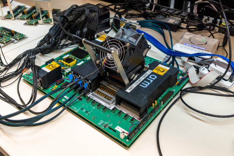
The Functional Validation Board does almost exactly as it sounds. Its purpose is to take an Arm AGI CPU and provide high-quality connectivity.
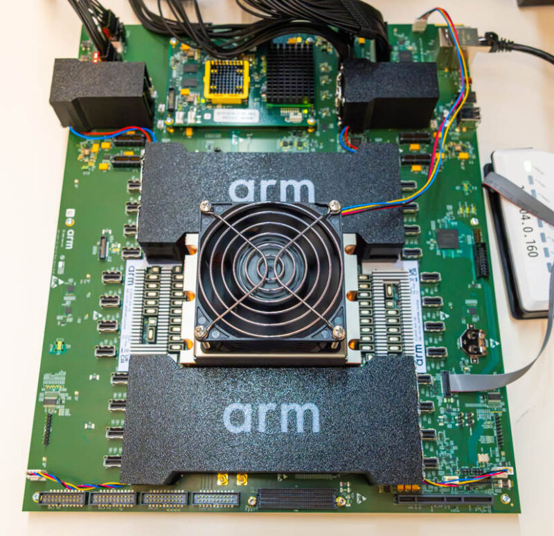
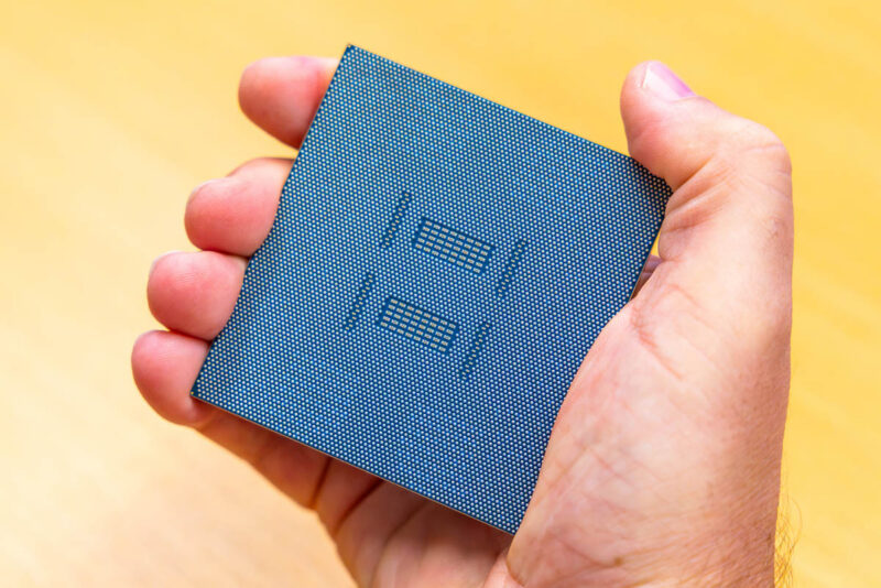
Put another way, for those who have never held a modern CPU, each of these pads on the bottom of the AGI CPU has a function to get a signal or power in and out of the CPU package. We usually talk about the inside of the CPU as having tens of billions of transistors, often proven in FPGAs before tape-out. Once the chips are manufactured, you need additional validation to confirm that what you sent to manufacturing works. Part of that is the internal workings. The other part, and a major reason for the Functional Validation Board, is to test that functionality communicating with the rest of the system. You need to know lower-level performance, like answering whether power is being delivered properly, whether the PCIe lanes work as intended, and whether the memory channels work.
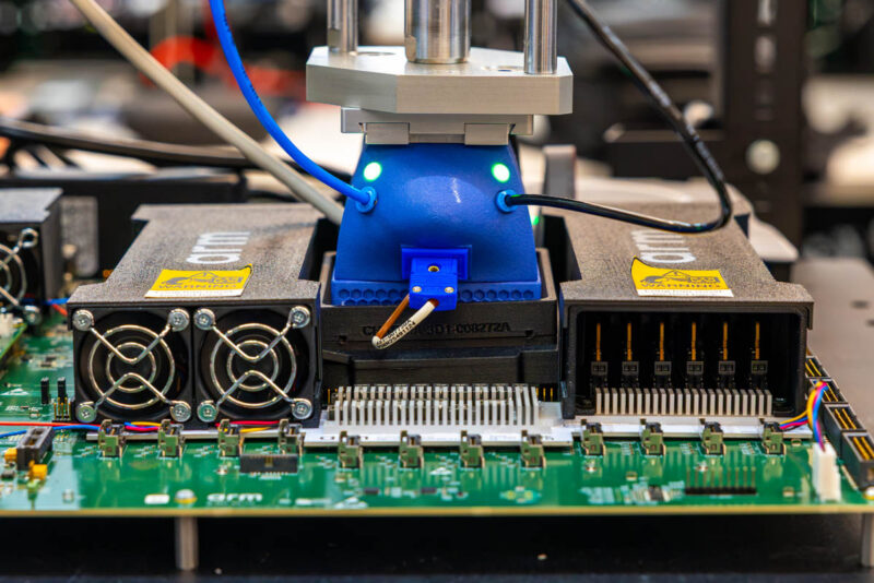
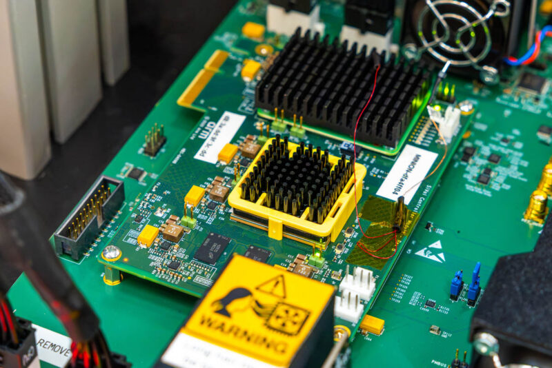
Once you have the board, you also need to do thermal testing to ensure the package performs as expected. Swapping chips in and out and testing how the chip behaves means that there are a lot of fascinating tooling bits around these Functional Validation Boards.
You can see that the PCB for these is thick, using a material you would not use for mass production. Likewise, the form factor is not designed to fit in a rackmount server.
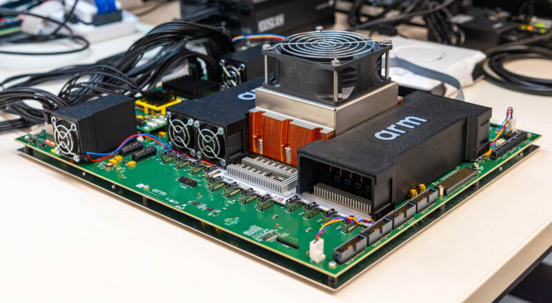
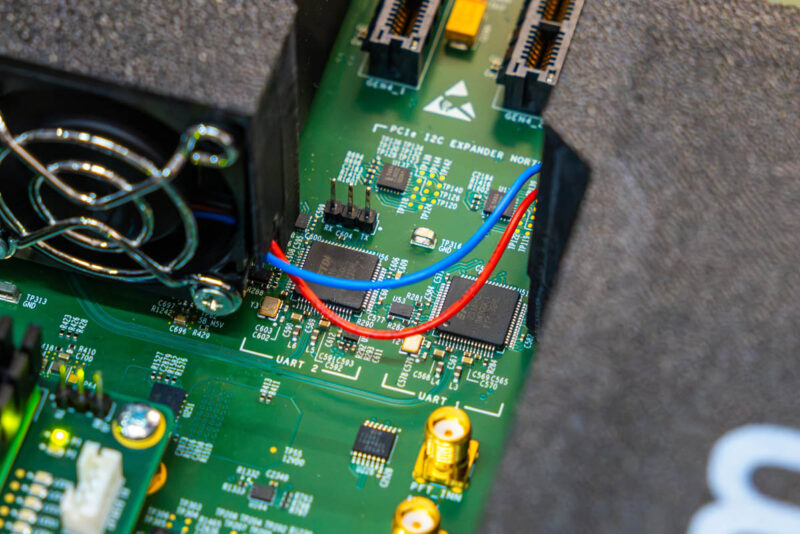
Connectors are spread out as well to make it easy to plug things in. While there are standards in the industry, it is not uncommon for there to be grey areas or devices that, in some cases, do not conform to specs. That is why you need to do extensive chip testing, as well as interoperability testing with memory modules, SSDs, NICs, GPUs, and more.
You can imagine the challenge. Sometimes you only have a single system to work with, or a handful. You need to know as soon as possible whether the first chips work so you can enter higher-volume production quickly. That first chip, and those first few chips, are the only ones in existence that you can test everything from the chips themselves to all of the components that can be plugged into a system. Then there is the BIOS and firmware work, OS work, application work.
One great story we captured in the video was of this first chip and platform. These are so important that they are often hand-carried. Sometimes the boards need to be carried in luggage. Engineers spend many months of their careers designing these chips, so when the first one comes in, with the first board to test it, they are often immensely valuable, as is every minute with the new hardware. As a result, sometimes the air parcel carriers do not do the last-mile delivery, and engineers go to pick up the parts at the terminal.
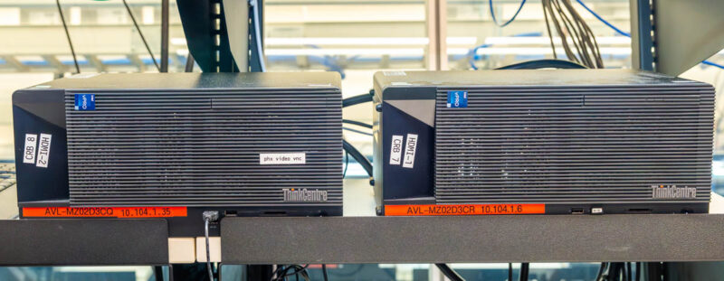
The ATE lab also includes machines that allow remote access. Teams from around the world need to access the systems to do their testing and fix any potential bugs. The hardware in this lab starts off scarce, so it is important to use it all the time.
Once the basic functional validation is done, and more chips arrive, the AGI CPUs are put into servers where they can be tested in a more real-world environment. That meant moving into a lab that was considerably louder, though we managed to keep it just below 100dB.
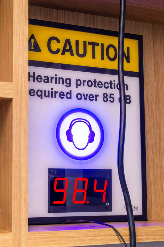
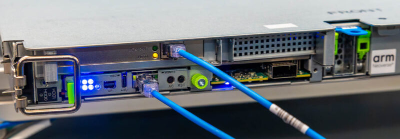
For folks unsure whether these chips are working, we saw them running not just on the validation boards, but on OCP-style server platforms.
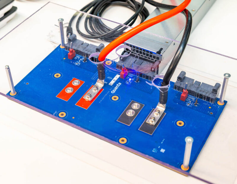
Arm even had the solution I have been trying to get for STH for quite some time. This is an AC power supply to an OCP busbar power solution so that Arm can power these servers.
Inside the lab, we can see the servers, in this case running side-by-side as two single-node systems in 1OU.
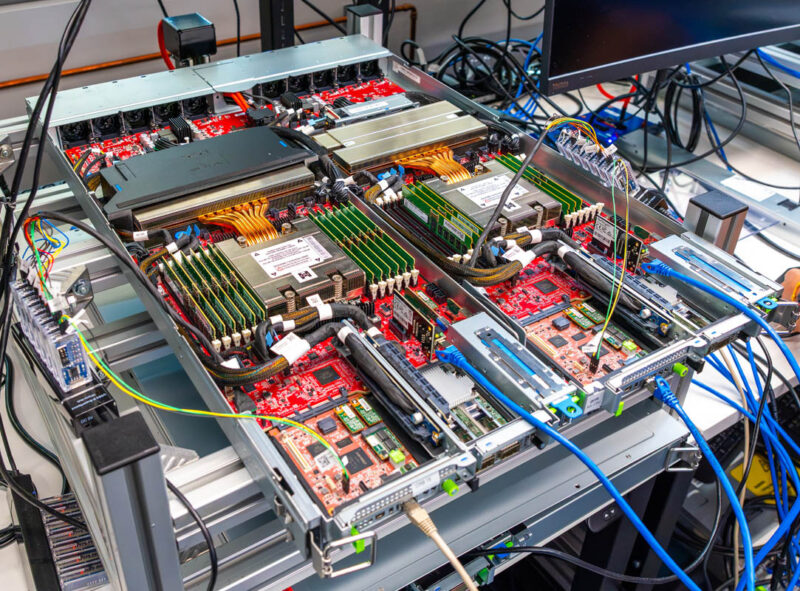
Here you can see the heatsink for the Arm AGI CPU along with twelve channels of DDR5 memory.
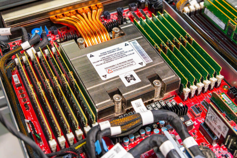
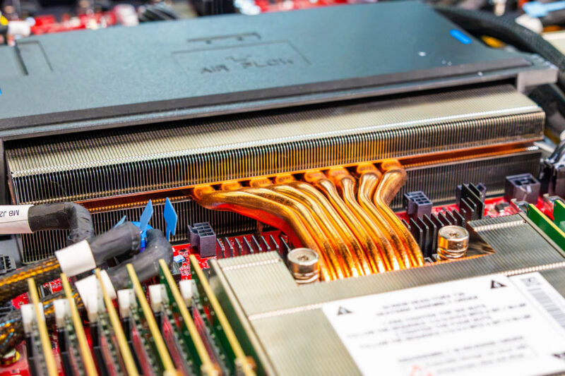
You may have seen these large coolers at STH when another hyperscaler sent us another one from our old set. These huge coolers, even for relatively modest TDP CPUs, let fans run at lower speeds in the data center. That, combined with the lower TDP also helps power consumption and TCO even in air-cooled servers.
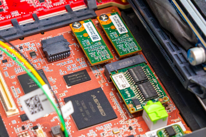
These were prototype servers, but still very functional, even with ASPEED BMCs as we would expect. ASPEED BMCs usually use Arm Cortex series CPU cores as well.
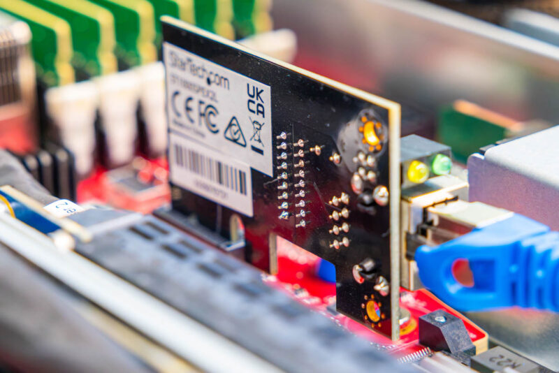
As much as these look like standard servers, there are a few differences specifically for lab instrumentation, like the inexpensive PCIe NIC in this system.
Or the odd bank just to get more access to the system that is being tested.
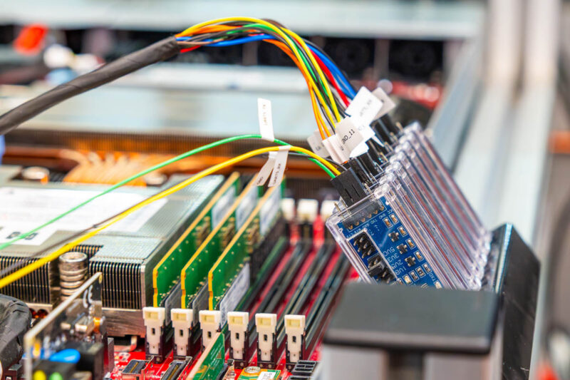
Overall though, these are next-generation server platforms up and running. For those wondering whether Arm will really have chips in 2026, I can tell you I saw them running live operating systems in OCP servers this summer.
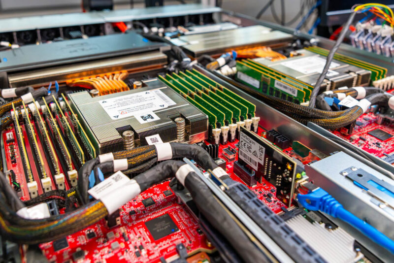
Still, this is a really great example of why building an entire CPU is very different from the Neoverse and Neoverse CSS designs. Instead of work stopping at the point of having IP, Arm needs to fabricate the parts, and then bring them up in-house and test them.
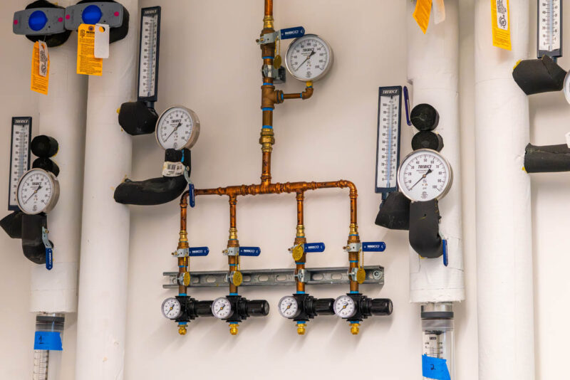
That may seem trivial at first, but this work can take months before customers get their parts.
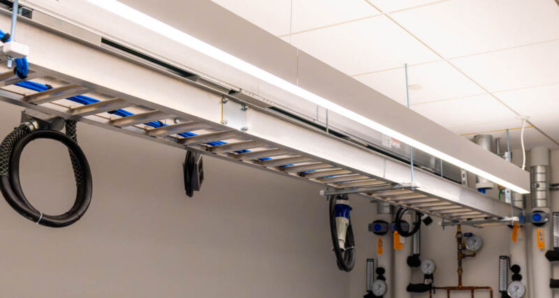
Also, once production motherboards and servers are ready, this lab can test those platforms.
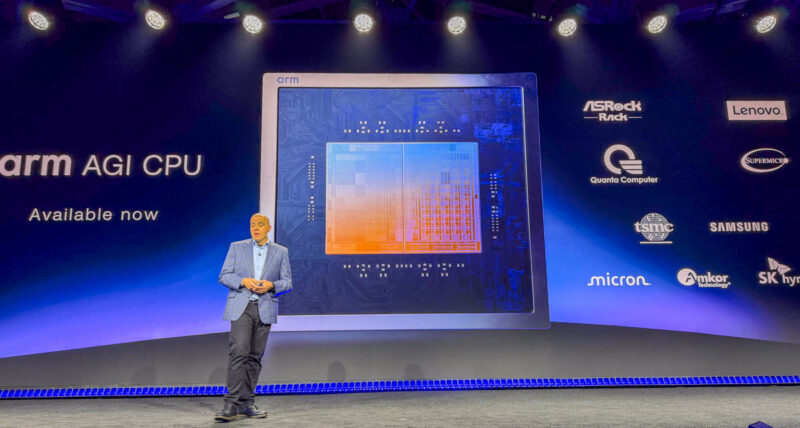
We caught the lab during a transition to a newly renovated facility as Arm prepares to bring this generation up. The reason Arm is building bigger and better facilities is that this is just the first-generation product. Arm has already discussed plans for several future generations of the parts.
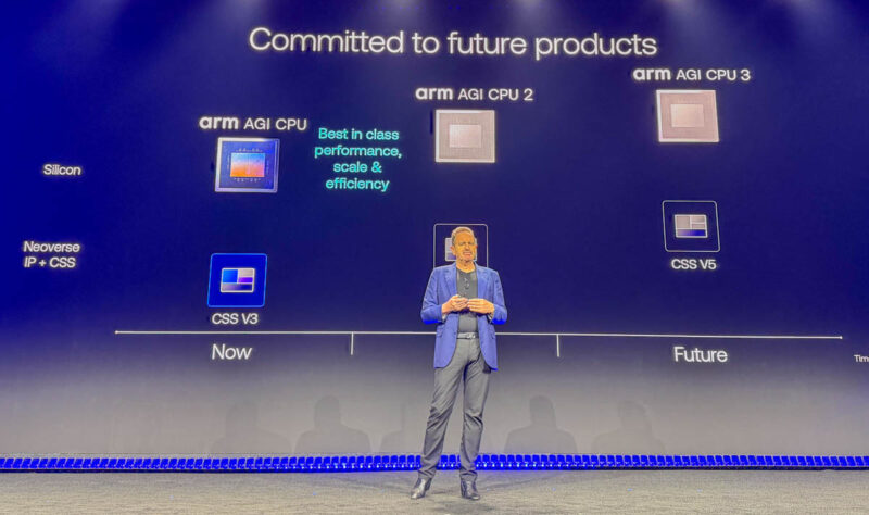
The goal is really to provide that choice, from just getting a Neoverse core to Neoverse CSS and all the way to a complete AGI CPU. Making the AGI CPU is now feeding back into Neoverse development. Since Arm is going through the process all the way to a shipping product, it can directly validate its simulation/ emulation against its own hardware and help customers to see how close its modeling work is to reality. Also, by bringing up hardware, teams across the industry gather key lessons learned that feed back into future development.
Final Words
When Arm mentioned they wanted us to do a tour, I was not quite sure what to expect. Once we arrived, I quickly realized that this is really the answer to the question of why a company cannot just buy a Neoverse core and ship a product tomorrow. Work has to go into tying those cores together and to the rest of the system. Then, once a chip is designed and manufactured, it is still a long road to validate what was manufactured and make it useful to many customers and within the broader server ecosystem. In some ways, that is why what Arm is doing is quite interesting. The AGI CPU is not just a CPU for a single customer. A hyperscaler building its own CPU can, for example, limit interoperability testing to its own needs. Arm is making the AGI CPU so Meta can use it, but also so you can buy a Supermicro server with the CPU.
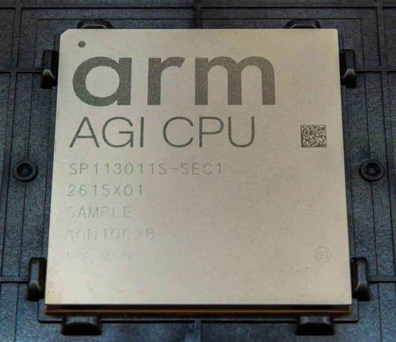
Making a CPU that can be used by many customers, just like a Neoverse IP, or Neoverse CSS can be used by many types of customers, means that Arm needs to move out of just the IP design and do physical engineering and validation work. We have been following Arm-based server processors for over a decade at this point, and seeing Arm take this next step, ranging from relatively lower-level IP all the way to a finished server CPU, is fascinating.
Hopefully we can get one of these in the lab soon, as we are starting to test new PCIe Gen6 servers and platforms right now. Arm’s goal is to provide a platform optimized for power-efficient computing, and it is approaching it differently than some other players in the market, which makes the AGI CPU promising, especially as the server CPU market grows so rapidly. Finally, I just wanted to point out that this is one where I know folks reading this are probably STH readers, but for this lab tour series, the video has other angles and tidbits that we just cannot fit into a written version. If you do not normally watch STH YouTube and read instead, this might be one worth watching, like our other on-site content.