
Microsoft publicly released the first Intel Skylake-EP Purley platform motherboard this week as part of its Project Olympus platform. The company is releasing the motherboard specs which can be found on the Open Compute Project website. Microsoft calls this its next-generation platform which from Intel roadmaps we know is Skylake-EP. By publishing this specification, Microsoft also released a slew of new information on the upcoming Purley platform that was previously confidential. At STH, we have seen several next-generation motherboards but we have abided by Intel’s embargo by not publishing pictures of said platforms as those were in closed-door sessions. This seems to be one of, if not the first sanctioned set of information on the Purley platform although Microsoft did go through some steps to hide the platform.
Microsoft Project Olympus – The First Publicly Available Purley Platform
Here is the picture of the actual platform. You can see that black areas were added to mask the DIMM configuration. Since the specification was released, we can easily find what is under those blacked-out areas.
On page 4 of the motherboard specification, we can see two rectangular CPU areas (more on that later) along with multiple DIMM slots corresponding to the blacked out areas on the above photo.
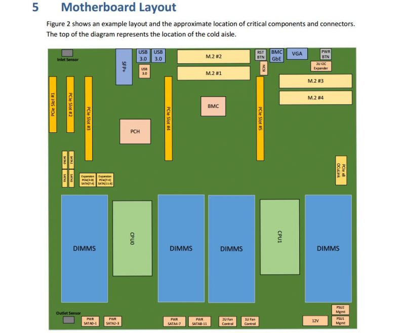
Page 3 of the document lays out key features so we can learn the exact configuration. Key features of the motherboard include:
- Support for up to 2 CPUs
- Support for up to 32 DIMMs
- Support for up to 12 SATA devices
- Support for up to 3 FHHL PCIe x16 slots
- Support for x8 PCIe cabling (OCuLink)
- Support for up to two PCIe x8 slots each capable of supporting up to two M.2 modules through an interposer board
- Support for up to four M.2 modules via direct-attach to motherboard
With 32 DIMMs that means there are up to 16 DIMMs per CPU. We also see support (page 14) on the motherboard for NVDIMMs in each slot. There are certainly (more than a few) things that stand out on that diagram, especially with the accompanying block diagram on page 3.
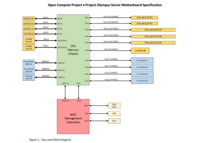
First, one can see a clear omission, the SFP+ connector needs a PHY. Without mention of a controller, one might assume that it is using a PCH derived PHY. Furthermore, adding lanes on the right hand of the page 3 diagram gives us a total of 88 PCIe 3.0 lanes. Grantley only supports 80 lanes between the two LGA2011-3 processors. Furthermore, one can see that there are two x4 Mini SAS HD connectors that are noted as being both SATA and PCIe. This is likely due to a flexible I/O technology allowing either to be used.
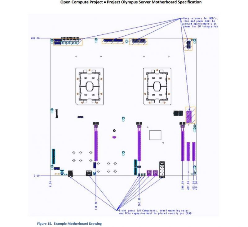
Of course, the next question is around sockets. The sockets we see diagrams of on page 31 of the document. Those rectangular sockets look like something we have seen on STH.
Here is a video of the Intel LGA 3647 socket from an already released Knights Landing platform. You will notice the same dimensions and the same octogon pattern at the center of the socket both in Microsoft’s OCP diagram as well as the Knight’s Landing LGA 3647 socket.
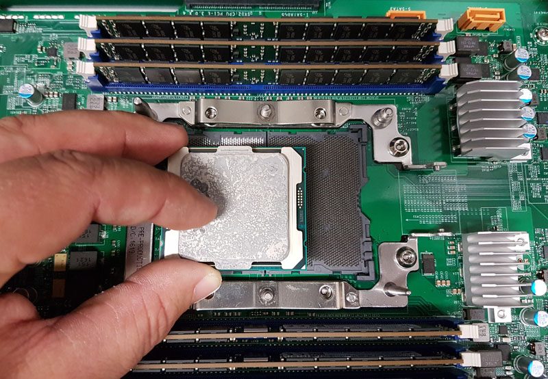
For comparison, here is the LGA 2011-3 “Broadwell-EP” chip atop a LGA 3647 socket.
Final Words
Much of this is expected as Purley is already deployed with Intel’s hyper-scale customers and there have been plenty of leaks thus far. Hyper-scale customers such as Google, Facebook, Microsoft, Amazon, Baidu and others make up such a large portion of the overall server market these days that it is not surprising we are seeing Microsoft debut a Skylake-EP platform well before we will see an official launch from Intel or its traditional server partners such as HPE, Dell, Lenovo, and Supermicro. Perhaps a harbinger of things to come as the hyper-scale players are publicly announcing Intel product many quarters before the company officially shares details to the public. At least we now have the first concrete system based on Intel’s next-generation server platform.
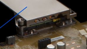
If you are looking for a Skylake-EP shot, here is an enlarged version of the picture on Microsoft’s site. You can see the Skylake-EP chip in there:


I do find it worrying that so called Hyperscale customers now get first crack at everything well before the smaller competition. It kinda feels like the old days when you had to buy your hardware through some large organization (Sun, IBM,etc.) or get cheap commodity hardware and rig it yourself, however there is no more cheap commodity hardware.
I wonder at what point Intel will switch memory technologies to something like HBM or HMC, or perhaps a hybrid model.
Comments are closed.