
At Hot Chips 29 (2017) Google presented a case study about their legacy TPU ASIC. The Google TPU is a custom PCIe accelerator for deep learning inferencing. The project was completed in around five quarters, very fast for custom silicon. Google discussed a key learning around memory bandwidth and what would have happened if they had used GDDR5 instead of DDR3.
Google TPU Background
The basic premise of the TPU is that it is a PCIe accelerator, much like we see GPUs or FPGAs when used as accelerators.
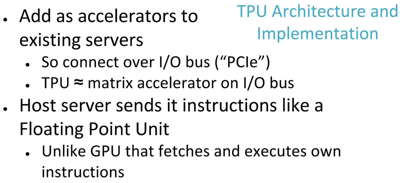
Specifically, it is designed for fast matrix multiply, important in deep learning applications.
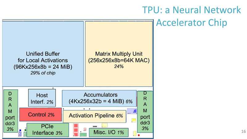
Here is a view of how much logic is dedicated in the chip to different functions:
To the programmer, Google is providing a view in terms of what using the TPU looks like.
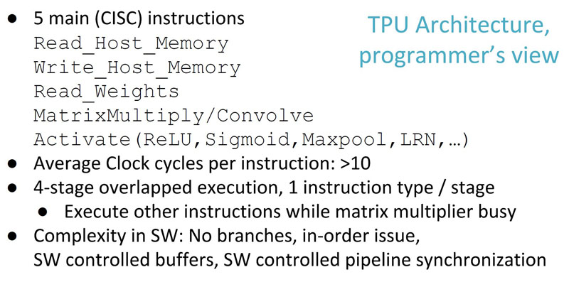
The TPU has only 11 instructions, five are commonly used. It is an in order design that relies on software to handle complexity.
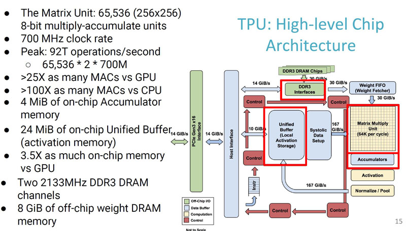
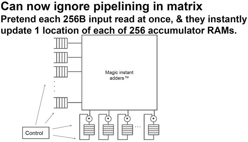
Google is focused on systolic execution in the TPU:
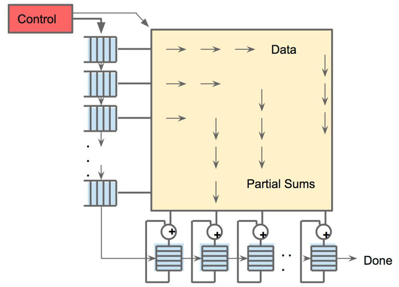
Memory bandwidth is extremely important in the architecture so the TPU is designed to efficiently move data around.
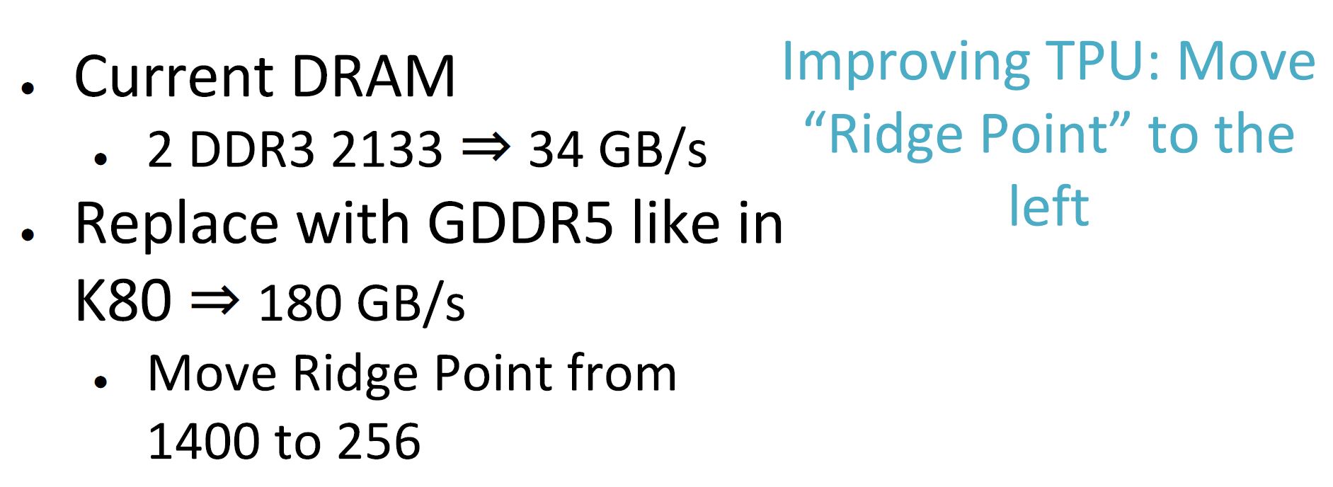
In this architecture, Google’s TPU team found that they are limited by memory bandwith. As a result, the team modeled what would have happened had they used GDDR5 instead.
What if there was a Google TPU (v1.1) Update GDDR5 for Bandwidth?
Google used DDR3 in its original design. One option was to move to DDR4 for higher bandwidth operation. Another potential design decision was to move to GDDR5 which is what Google showed at Hot Chips:
The company explained that they were not necessarily compute limited in their original design. DDR3 was too slow. Here is what Google is claiming if the TPU had GDDR5 in terms of performance per Watt:
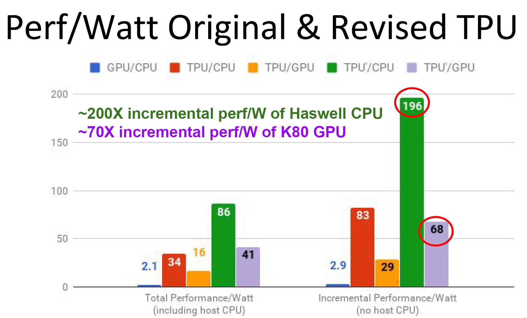
The key here is that the GDDR5 version would have had more bandwidth and lower latency boosting performance. Instead of building the v1.1 version using GDDR5, Google leapfrogged GDDR5 and moved to HBM for its TPU v2 which could also be used for training, not just inference.
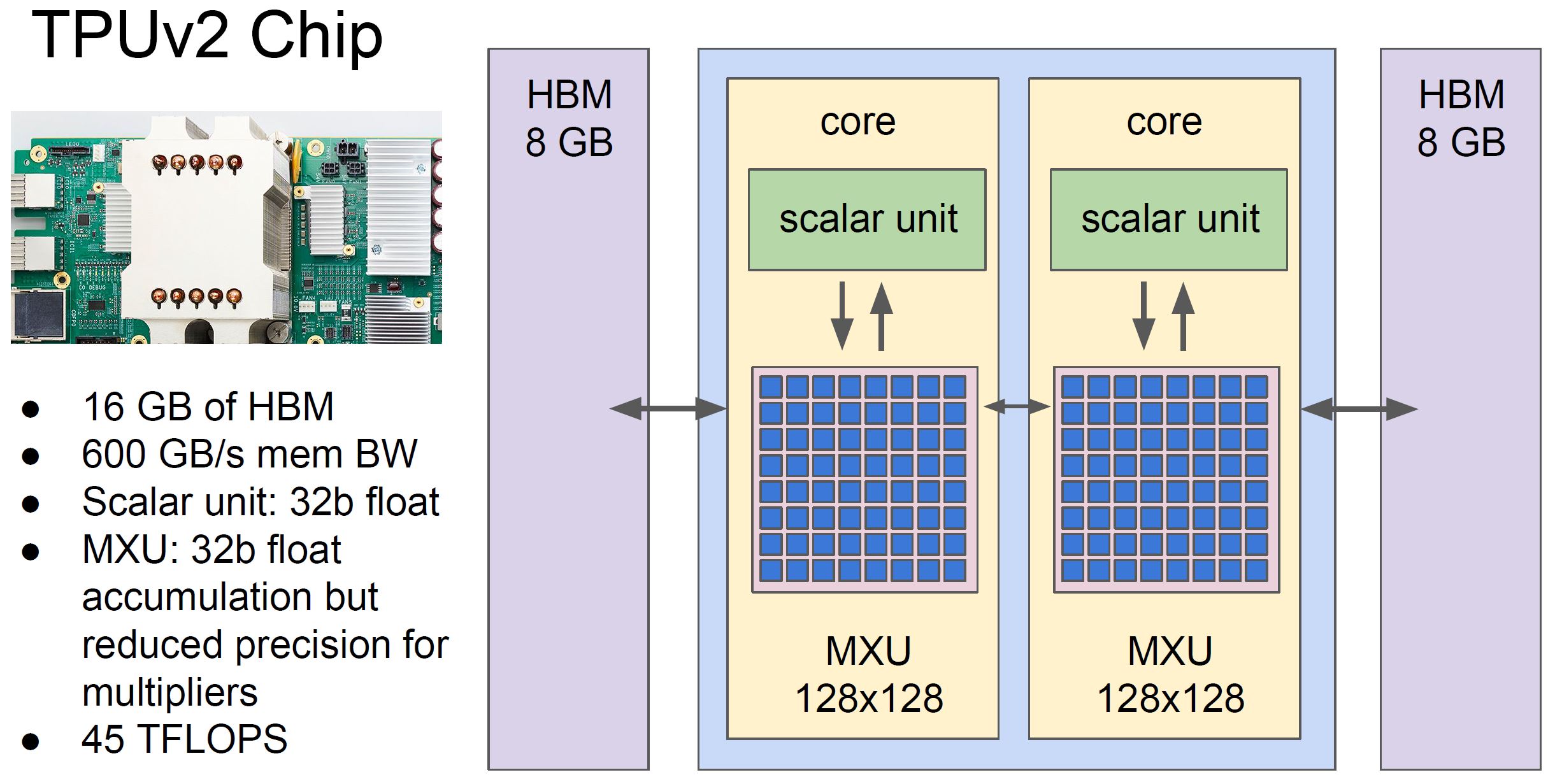
Cloud TPU v2 Architecture
How Google actually followed up the TPU is with the TPUv2. Instead of updating to higher bandwidth GDDR5, Google is using even faster HBM in 16GB capacity. That gives them 600GB/s of memory bandwidth. For comparison, that is about four sockets worth of AMD EPYC.
Here is what the Cloud TPU v2 Looks like with four of those blocks combined:
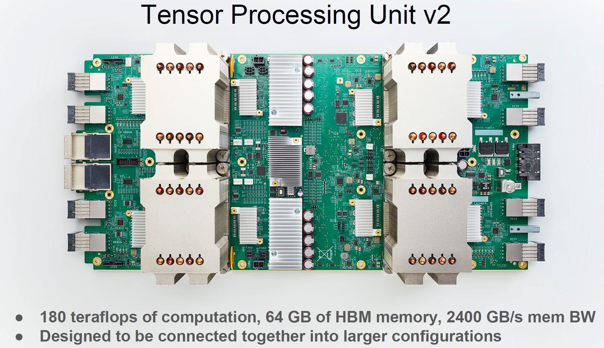
These are the much larger compute units with more TDP headroom that Google is making available to developers.
Final Words
While this is a study in an older generation product, it is still interesting from a design standpoint. One area that we would like to see Google’s TPU team move the ball forward on is their comparisons. While the K80 may have been excellent years ago, and is still widely deployed, it is now three generations old as NVIDIA Tesla V100 Volta is available. At the same time, the key takeaway is that the large hyper-scale players are building their own hardware and topologies well beyond simply adding a GPU to a server.


 attendees were treated to a case study on the original Google TPU and what the TPU would have looked like with GDDR5)