
Today’s regularly scheduled article (part of a series at STH that was set to launch) had to get pulled for re-testing. This has been a busy week where a lot of the editorial team is on PTO so we thought about what could be fun to show. Here is the AMD EPYC 9004 “Genoa” de-lidded so we can see what is underneath the normal heat spreader.
AMD EPYC 9004 Genoa Under-the-Lid
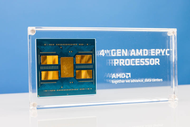
Normally when you see an AMD EPYC 9004 series CPU, it looks something like this.
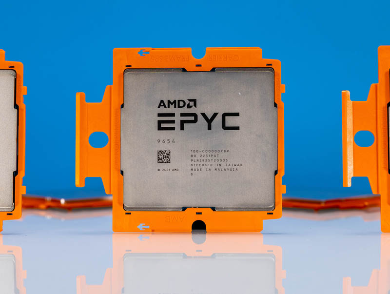
Around the CPU, there is an orange socket guide and then there is a large metal heat spreader atop the CPU to distribute the heat away from the silicon packages and to the thermal solution.
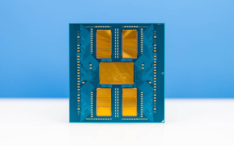
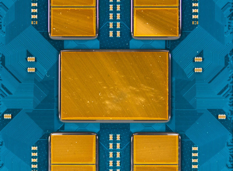
Here is what that chip looks like without the orange socket guide and heat spreader lid.
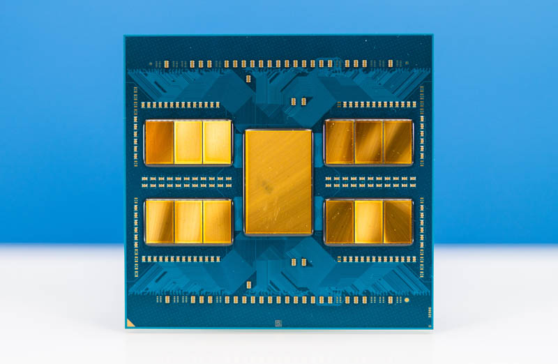
In the middle is an AMD EPYC 9004 I/O die. Around that I/O die are twelve CCD packages each with up to 8 cores and associated caches.
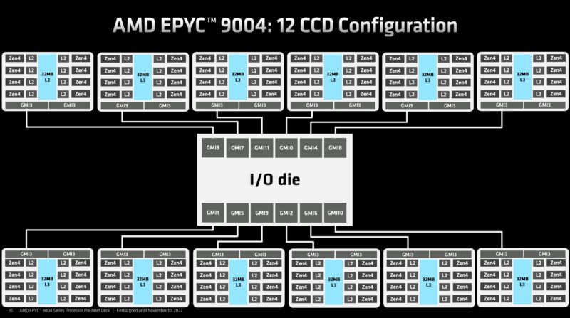
The diagram above is the slide version, but if this helps, here is the EPYC chip rotated so the I/O die is oriented as it is in the slide.
That I/O die connects the twelve CCDs, twelve memory channels (and in theory, 2DPC), 128x PCIe Gen5 / CXL 1.1/ Infinity Fabric lanes, and the miscellaneous extra PCIe Gen3 and other lanes onboard.
While looking a the CPU when it has its lid on top may look like a simple hunk of PCB and metal, but underneath the lid, there is a lot more going on.
Final Words
At the pre-brief event for the AMD EPYC 9004 series, we had a number of photos of de-lidded chips, as we have here. According to Patrick, who was at the event, those photos were apparently removed by someone borrowing the Canon R5 we primarily use for photos (always back up before handing a camera over.) Still, we were able to grab the photos when we took apart a display case:
Hopefully, our readers think this is a fun look at a massive chip. This is also a look at what is to come as multi-chip packages become the norm. In a few years, we will not see a 13-die CPU as an engineering accomplishment. Today, this is one of the most advanced CPUs in the world.


I wonder, has anything newer than Zen 1 landed on Epyc Embedded? I remember the single die versions rolling out, then the dual dies, but they still had the monolithic designs. Xeon D too hard to compete with while making enough on the chips?
I see some capacitor pads aren’t populated. The 9654 is a top-of-the-line, high-current part, why on earth would there be pads unpopulated?
@ssnseawolf: Could those be to support the extra cache that Genoa-X parts will have? AMD seems to be going aggressively modular lately, so they’d probably be much happier leaving a few extra pads than they would having to do a second substrate variant if it can be avoided.
@fuzzyfuzzyfungus Excellent point. I figured Genoa-X would be a different socket with more pins, which may have been an incorrect assumption.
So far there have been two chips announced for SP5: Genoa (with Genoa-X being a variant) and Bergamo. I suspect that Bergamo will leverage a different substrate and CCX dies than Genoa but utilize the same IO die. Thus socket compatibility between Genoa(-X) and Bergamo is maintained. What is interesting is that Bergamo is only going to 128 cores presumably across eight 16 core CCX dies but the IO die has the potential to link up to twelve CCX dies. Power consumption is one factor and area on the substrate are two potential factors but both don’t seem the real issue.
AMD also has SP6 due at the end of the year for a cost reduced platform for telco/workstation. This is moving the Genoa(-X) CCX, Bergamo CCX and the IO die into a different form factor with less PCIe lanes and memory channels.
Everything will again change with Zen 5 but that is a 2024 product from all accounts. The big change I would predict is a move to a die-to-die schema using EMIB-like technologies. IO gets split and moves around the CCX dies in a pseudo grid. The result is that core count scaling becomes limited by power and size on the substrate for existing sockets. I would predict that this is also the generation that we get to see on package FPGA and/or RNDA/CNDA compute.
SP6 will first use Zen 4c cores so only 4 chiplets, apparently the customers request for a 64 core and they don’t need that much cache.
Other zen 4 configurations for SP6 is yet unknown. And yes, Bergamo will use 2 links per chiplet. There are more GMI links left on the IOD.
More cores per chiplet requires more bandwidth, and Bergamo chiplets are slightly bigger than zen 4c so fitting 12 is impossible anyway although zen 4c is almost twice as dense
Comments are closed.