
Qualcomm this week presented new details around its upcoming ARM CPU. We had a lot of interest around the Qualcomm Centriq 2400 after the company’s Hot Chips 29 presentation. At that time, the company did not disclose key facts such as clock speeds and cache sizes. This week, Qualcomm presented new facts on the Centriq 2400 10nm chip design.
New Qualcomm Centriq 2400 Details
Here is the Centriq 2400 overview from Hot Chips 29. We now have more details around some of the specifics.
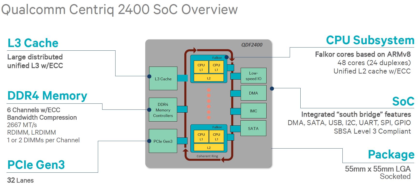
First, in terms of clock speed, we can expect 2.0GHz+ clock speeds out of the chip. Clock speed impacts both performance and power consumption so going above 2GHz provides some sense regarding where that will end up.
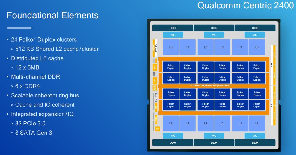
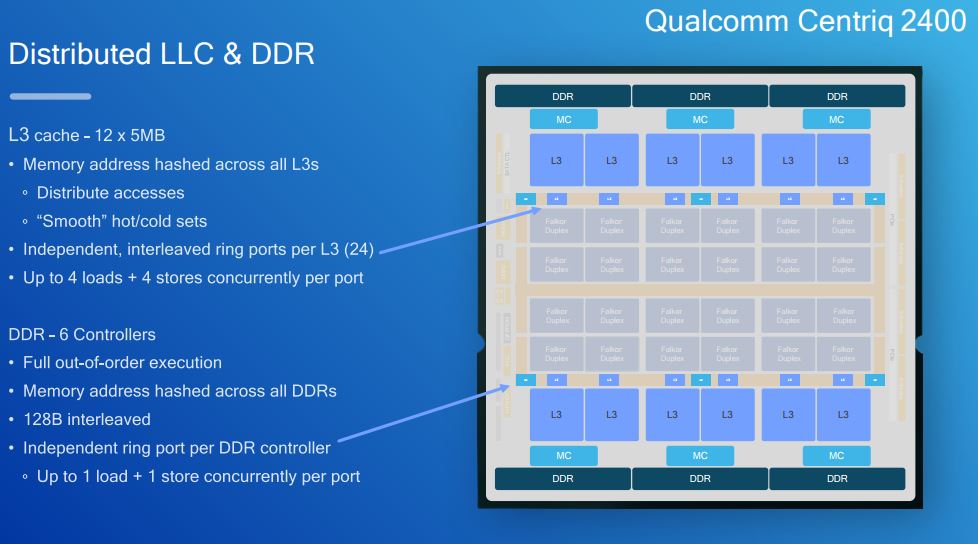
Also new are the details around the interconnect and L3 cache sizes. We can see a total of 60MB L3 cache is listed. L2 cache size is listed as 512KB shared per cluster with 24 clusters gives us a total of 12MB L2 cache.
The inclusion of 8x SATA III 6.0gbps ports helps us see where this is targeted. A larger SATA array would have made us think this is a storage application focused chip. 8 SATA III ports makes sense as we are seeing a bigger focus on NVMe for primary storage with 1-2 boot SATA III devices being common. SATA III is quickly becoming the interface of choice for commodity hard drive storage.
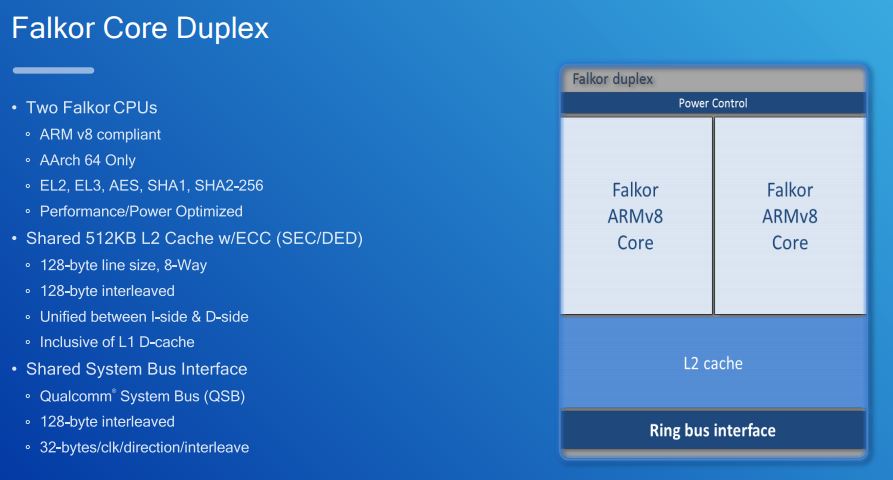
We had a lot of this information about the Falkor Core Duplex from the Hot Chips presentation, including details such as this is AArch 64 only. The 512KB L2 ECC cache is a net new add in this disclosure.
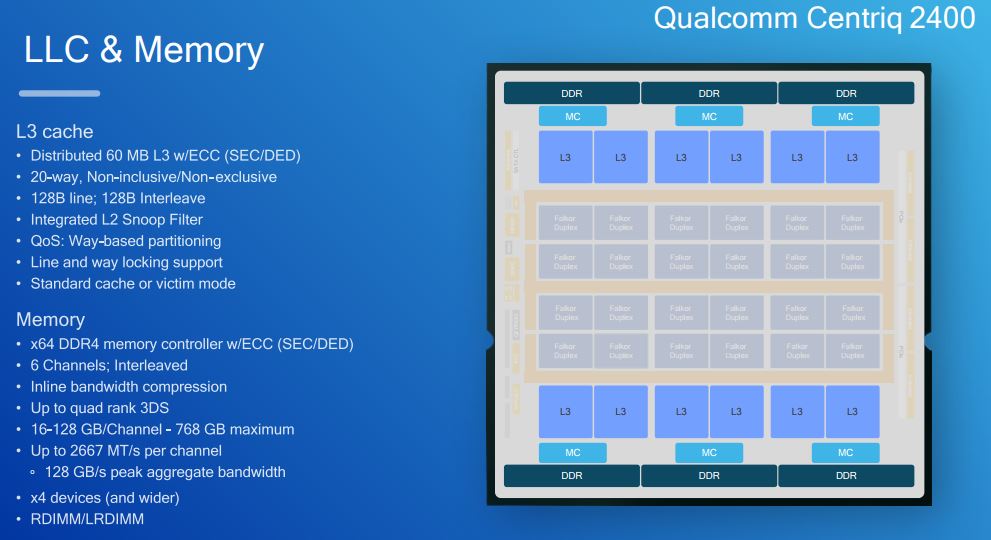
The L3 cache details are fascinating. There is a distributed 60MB L3 cache that is split into 12x 5MB chunks. The cache can operate in standard or in victim mode.
The on chip interconnect is a bi-direction segmented ring bus. It also is a multi-ring design. Some may compare this to the rings that we saw on the Intel Xeon E5 series. We see this as substantially different.
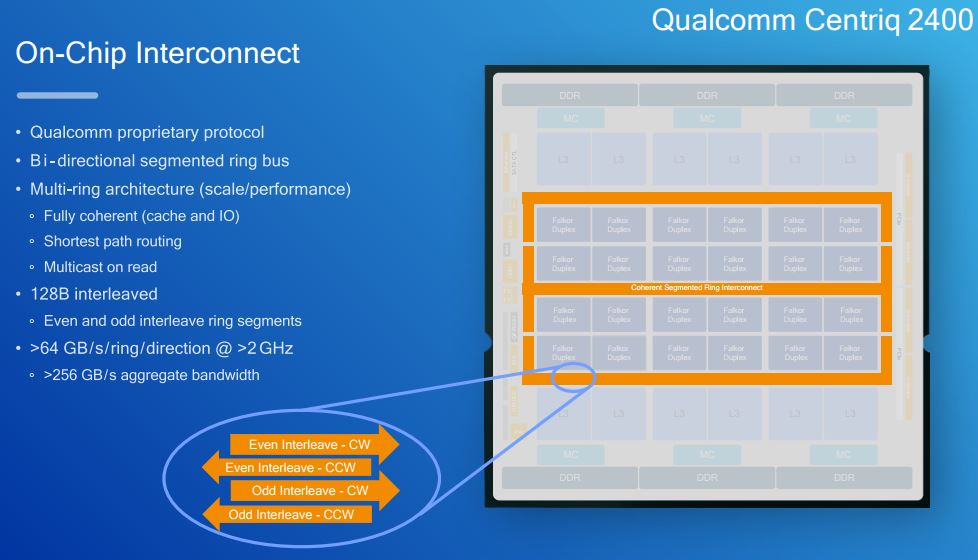
Each of the four ring segments has 64GB/s of bandwidth for an aggregate of 256GB/s.
Along these rings there are the 12x 5MB L3 cache chunks as well as the 6 memory controllers that support up to DDR4-2666.
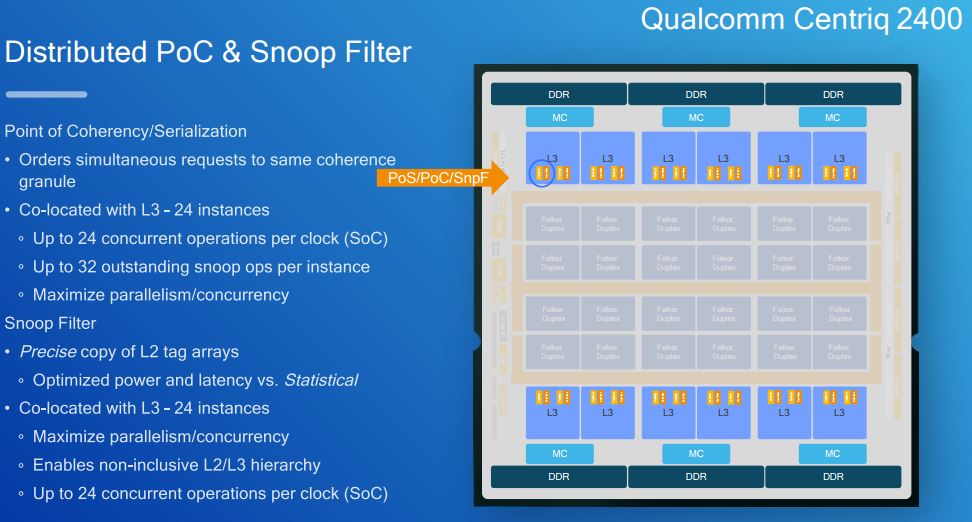
Dealing with the large L3 cache chunks and ensuring they are used efficiently by a large number of cores means that Qualcomm has to do a lot of work managing how data utilizes the space.
As a bit of perspective here, Qualcomm has more combined on-chip L2 / L3 cache than the $10,000 Intel Xeon Platinum 8180. That is a huge amount of silicon real estate dedicated to cache.
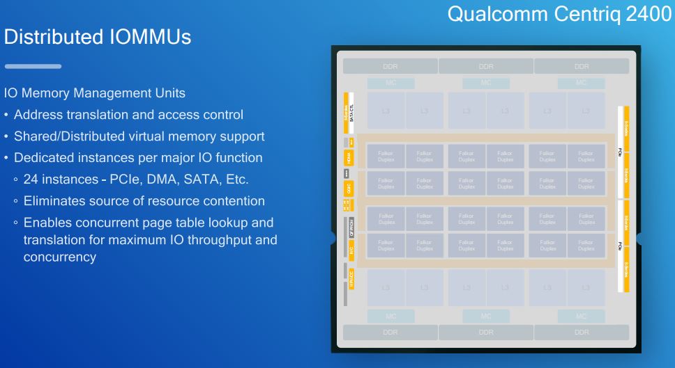
The distributed IOMMUs help Qualcomm manage resource contention. Our sense is that the Qualcomm Centriq 2400 was intended to have a significant amount of I/O devices connected so this is a major design point.
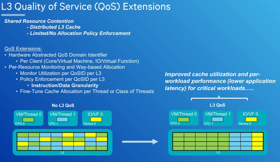
The L3 Quality of Service extentions we covered in the hot chips piece. The updated slide is slightly different so we are just going to post it for our readers.
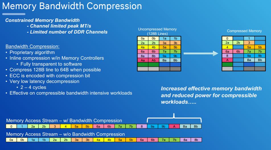
The memory bandwidth compression slide is the same as we saw at hot chips, save some formatting. Memory bandwidth compression is a key technology that Qualcomm is using to compress data inline with low latency.
Final Words
Overall, we are pleased to see that Qualcomm will have higher-clock speeds. The Cavium ThunderX topped out at 2.5GHz and we are hoping for high clock speeds on the Qualcomm Centriq. High clock speeds help with latency sensitive requests. We are impressed by the sheer volume of L2 and L3 cache on the Qualcomm Centriq 2400 as 72MB combined L2+L3 cache is extremely aggressive in addition to having 48 cores on-die.
Stay tuned for more on the Qualcomm Centriq 2400 from STH.


I’d say this is promising. That’s lots of cache. I’m just as interested in hearing your input on usability as performance, maybe more.
Embedded dual 1GbE not even 10G? Why even bother? Is anyone really going to run these chips off gigabit ethernet?
I would’ve loved to see them do something cool with embedded 10/25/40/100 and that IOMMU and QoS stuff instead.
The hyper-scale guys all use their own NICs. Cavium learned this with ThunderX (1) which is one reason ThunderX 2 does not have 40/50/100GbE.
Isn’t ThunderX2 based off Broadcom’s Vulcan design rather than the original ThunderX2 presented a couple of years ago? Perhaps that’s the other reason for not having NICs on chip(?) because if it wasn’t originally on Vulcan, it might not make sense to add it.
That is true as well @dfx2
It seems quite light on I/O though with 32 PCIe lanes. PC HEDTs have more these days. I’m left with a feeling that they missed a few opportunities to go big. Unless, despite the talk of wanting to take on Xeon, they actually know they’ll realistically take on Atom at the fringes of the datacenter.
They’ll also have to share a roadmap… most server makers take that sort of thing seriously.
Comments are closed.