
Micron announced this week that it has started to ship its new generation of NAND. The new Micron 232-layer NAND means that the company is able to cram up to 1Tb into a single die using TLC. As this new NAND makes its way into products, it will lead to higher capacity or potentially lower-cost (at a given capacity) SSDs.
New Micron 232-Layer NAND Increases Drive Density
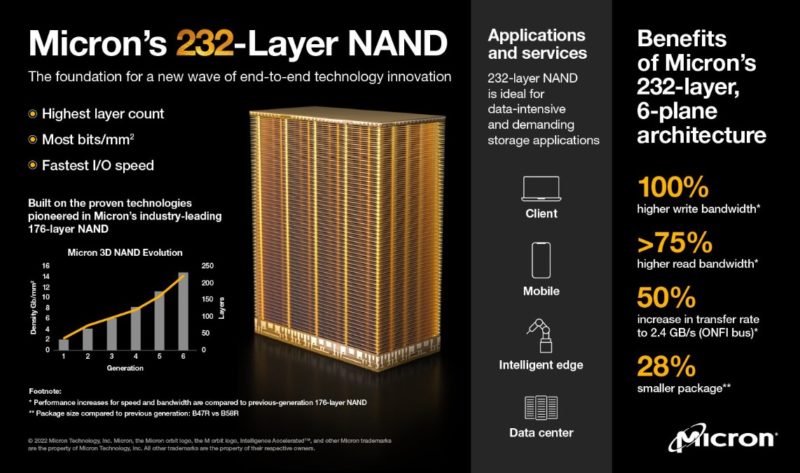
The new Micron 232-Layer NAND increases the planes per die and has new signaling methods. Micron says this is good for doubling write speeds and a 75% increase in read speeds. Increasing the speed per die is important as the dies have a higher density because each die can store more data.
Perhaps the bigger impact of the new NAND is that it will enable 1-2TB SSDs with a single package once 8-16 die stacks are created. With higher density packages, SSD designers can get to larger SSD capacities or simply build smaller SSDs. For the server market, this is the type of breakthrough that could lead to more M.2 2280 drives with PLP as capacity points can be hit with less space on the PCB for NAND. That is not a product announcement, but it is something we expect to see in the next few quarters from various vendors. That, along with EDSFF E1.S will put pressure on the M.2 22110 markets. It may also make smaller DRAM-less drives more appealing.
Final Words
Micron says it is shipping the new NAND. We will probably start seeing it in products over the next few months. We expect to see more products based on the NAND as new generations of drives hit the market. On the consumer end of the market, NAND gets swapped into existing models, but that is far less common in the data center and enterprise markets when 3rd party validation needs to take place.


It goes without saying that that what wasn’t said might be the most interesting. The slide is silent on thermals & endurance … and so is the blog article at Micron, too.
I was just thinking the same thing. It would be great of this TLC didn’t burn itself out 2 times faster as well… NAND SSDs Achilles heel, so to speak.
I wonder how long this takes to fab from start to end. If I recall correctly, it was measured in months even 2-3 generations ago.
A question I have is at what point will NAND chip density be great enough to where we won’t have to use TLC/MLC/QLC any more and we can go back to SLC for the purpose of improving the cycle life of SSDs? I have to assume that there will come a day when the density of cells will be such that continuing to use iterations of TLC and MLC will go by the wayside and SSDs will go back to using SLC instead, making them more in line with traditional hard disks, write cycle life-wise.
Will this result in larger M.2 drives or just more cost reductions of the current capacities?
Comments are closed.