
Meta has a new in-house AI accelerator for the company’s growing AI workloads. Dubbed the MTIA 2, or Meta Training and Inference Accelerator 2, the new chip has a different architecture than many of the newer parts we see, with some clear optimizations for scale-out.
New Meta AI Accelerator MTIA 2 Revealed
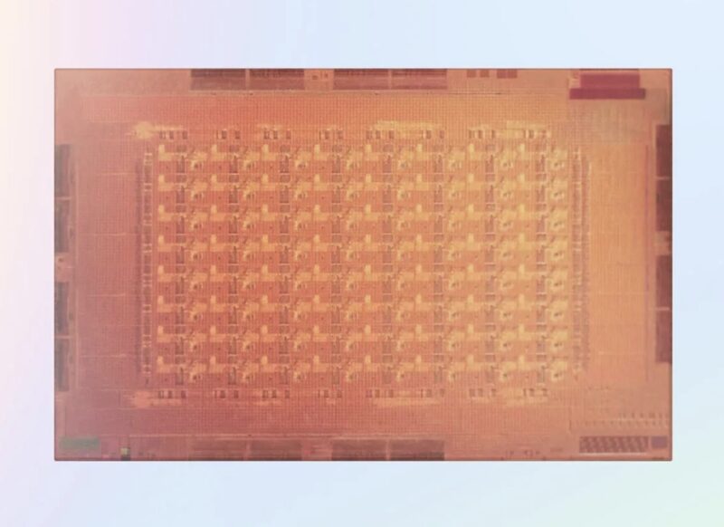
Here is the MTIA 2 die that is around 421mm2 on TSMC 5. Meta says that the die has around 2.35B gates.
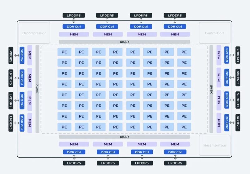
The chip is laid out with an 8×8 matrix of processing elements, or PEs at the center. On the outer edge, there are other features like the host interface, a memory controller for the LPDDR5 memory that sits around the accelerator, and the fabric. We can also see a control core and decompression engine on the diagram. At STH, we often discuss how much of a die is used for non-compute tasks. This is a great example since it is easy to see the PE versus non-PE area. It also shows just how much of AI-focused designs center around memory and data movement.
The MTIA 2 accelerators are packed into chassis and are very different than what NVIDIA is doing with its accelerators. Each board holds two 90W accelerators so it can be air-cooled. With a PCIe Gen5 x8 connection to the host, the two accelerators can share a x16 edge connector. There are twelve boards in each chassis for 24 per chassis. Meta says that it deploys these in sets of three for 72 accelerators with an option for an RDMA NIC. Whereas we usually credit AWS Nitro for the interest in DPUs, Facebook/ Meta made a major innovation years ago, deploying multi-host adapters at scale to lower networking costs. Here, the accelerator-to-NIC ratio seems to be much lower than that of NVIDIA systems.

Here are the key specs from Meta on the accelerator’s performance:
GEMM TOPS
- 708 TFLOPS/s (INT8) (sparsity)
- 354 TFLOPS/s (INT8)
- 354 TFLOPS/s (FP16/BF16) (sparsity)
- 177 TFLOPS/s (FP16/BF16)
SIMD TOPS
- Vector core:
- 11.06 TFLOPS/s (INT8),
- 5.53 TFLOPS/s (FP16/BF16),
- 2.76 TFLOPS/s (FP32)
- SIMD:
- 5.53 TFLOPS/s (INT8/FP16/BF16),
- 2.76 TFLOPS/s (FP32)
Memory Capacity
- Local memory: 384 KB per PE
- On-chip memory: 256 MB
- Off-chip LPDDR5: 128 GB
Memory Bandwidth
- Local memory: 1 TB/s per PE
- On-chip memory: 2.7 TB/s
- Off-chip LPDDR5: 204.8 GB/s (Source: Meta)
Something that stands out is the memory capacity to AI accelerator watt ratio. The LPDDR5 memory may not offer huge amounts of bandwidth compared to HBM-based accelerators, it offers relatively high capacity. Meta has something like 128GB of memory / 90W TDP for about 1.42GB/W. Compare that to the Intel Gaudi 3 we showed this week at 128GB of HBM2E and a 900W TDP that is 0.142GB/W. It is clear that Meta is targeting a different memory capacity to compute capacity ratio than many other chips we see.
Final Words
Meta’s post on MTIA 2 talks about hardware and software co-design. The company has big enough applications where it can make dedicated accelerators. It feels a bit like showing this off was less focused on the impact on production and more focused on being a recruiting tool. Meta has been a leader in AI, and buys a lot of compute and memory, so it makes a lot of sense that they are exploring different architectures.


Article says 708 TFLOPS/s for sparse INT8, while, for AI integer number tensor calculation arithmetic performance, TOPS is used.
TFLOPS means Tera FLoating point Operations Per Second, and it is used sorely for floating point number arithmetic. the last PS of TFLOPS means per second, so TFLOPS/s is redundant.
Comments are closed.