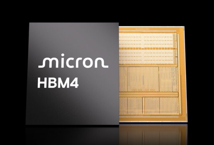
Today, Micron announced that it has started shipping next-generation high-bandwidth memory, HBM4. HBM is a key technology to enable today’s AI accelerators and HPC processors. Using HBM trades capacity and serviceability for speed, and that is why a new generation is a big deal.
Micron Begins Shipping HBM4 Memory for Next-Gen AI
HBM4 features a 2048-bit interface and now up to 2.0TB/s per memory stack. Remember, there are often several HBM stacks on a modern accelerator. For some reference, Micron HBM3E was something like 1.2TB/s so that is around 60% higher performance.
The first samples shipping to customers are 36GB HBM4 stacks, so chip designers can get capacity at the same points as HBM3E. Of course, we have seen other generations of HBM stacks get refreshes with higher capacities. With today’s LLMs demanding more memory capacity and memory bandwidth, HBM4 will be the answer for next-generation designs.
Micron also said that the new memory is built on its 1-beta process and has “highly capable memory built-in self-test (MBIST)” functionality. A notable challenge with HBM is that integrating the memory onto a complex package means that the AI packages need to be both fast, and reliable.
Final Words
Micron says that the HBM4 is now being sent to customers, but the production ramp will not be until 2026. As a result, this is not something that we are going to see today. Instead, they will ramp along with next-generation accelerators. As AI accelerators continue to get larger, having HBM continue to advance to higher speeds is important since accelerators usually have limited space to add stacks of HBM. Those physical sites often determine the memory bandwidth and capacity of a platform. In the future, we expect that we will see HBM combined with slower capacity tiers like LPDDR to expand memory footprints of accelerators even further than today.


Given that most of the bandwidth increase for HBM4 stems from doubling the width, there is another 20% improvement for just matching the clocks of HBM3E. Higher clock speeds are also expected, though I’m not sure how high they can drive things. That 2048 bit width per stack is a lot but subdivided into 128 bit wide sub channels. Even with the fine tracing possible, driving bus speeds higher at these sub channel widths is going to be a challenge.
The 36 GB capacity is done through 12 stacks of 24 Gbit dies. I believe HBM4 has provisions for 16 stacks with 32 Gbit dies arriving in the short term permitting a 64 GB HBM4 stack.
The real critical part for HBM4 is going to be the edge length. I have a strong feeling that designs are going to be basing chiplet size around the HBM4 edge length instead of attempting to build large monolithic designs leveraging multiple HBM4 stacks. Ultimately that’ll mean way more silicon inside of a larger package.
Considering that doubling the width is the primary driver of the bandwidth increase in HBM4, matching the clocks of HBM3E results in an additional 20% improvement. I don’t know how high they can drive things, but higher clock speeds are also expected. A stack with 2048 bits of width is a lot, especially when broken down into subchannels with 128 bits of width. It will be difficult to drive bus speeds higher at these sub channel widths, even with the precision tracing that is achievable.