
Sorry for the dense title. Today, Lightmatter is disclosing a breakthrough in its CPO (co-packaged optics) solution. The Lightmatter Passage 3D CPO now does 16-lambda DWDM (Dense Wavelength Division Multiplexing) on a single fiber. Lambda in this case is not the AI Neocloud that we just looked at in Exploring the NVIDIA HGX B200 Lambda AI Cluster at Cologix with Supermicro. Instead, it refers to wavelengths of light where data is being transmitted.
Lightmatter Passage 3D CPO Does 16-lambda BiDi DWDM Over a Single Fiber
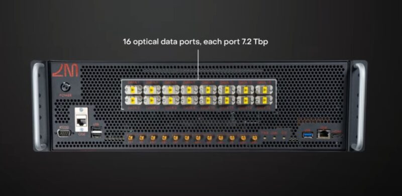
Lightmatter’s reference platform for its Passage has 16 ports, and each is putting out 7.2Tbps.
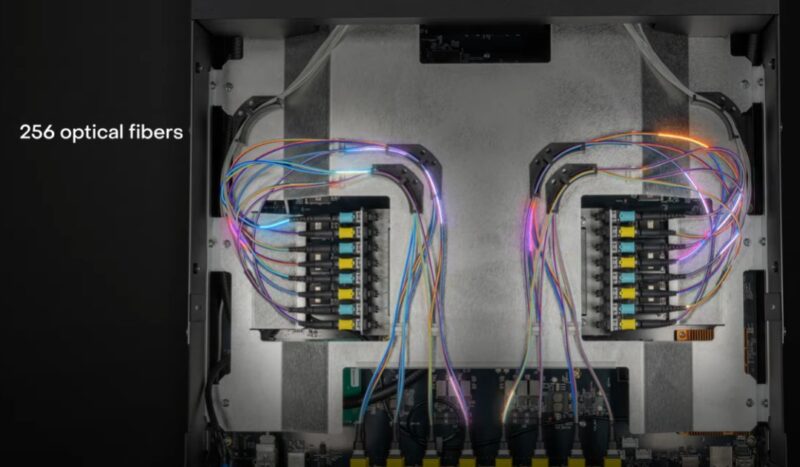
Those sixteen external ports go to 256 internal optical fiber ports on the reference platform.
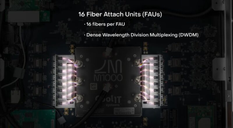
They attach to the 16 Fiber Attach Units or FAUs on the Lightmatter M1000 reference platform.
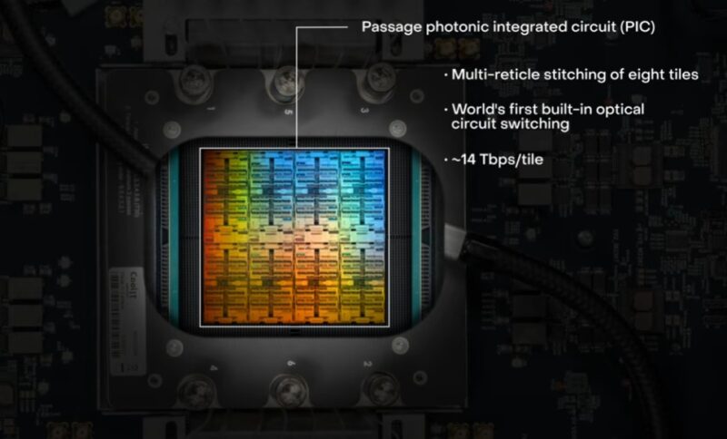
This is a silicon photonics implementation, so we have our PIC, or photonic integrated circuit, with eight 14Tbps tiles.
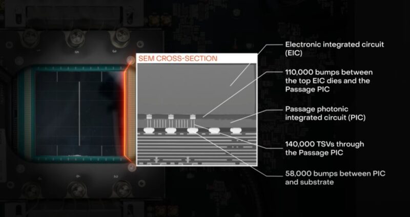
Here is a cross-section with the EIC and PIC and how all of those interact.
We did a bit of a lab demo on some of these parts of optical communications last year in our Going 800Gbps at up to 1000km with the Marvell COLORZ 800 piece. That is a different technology, but things like the PICs are shown there in a larger demo.
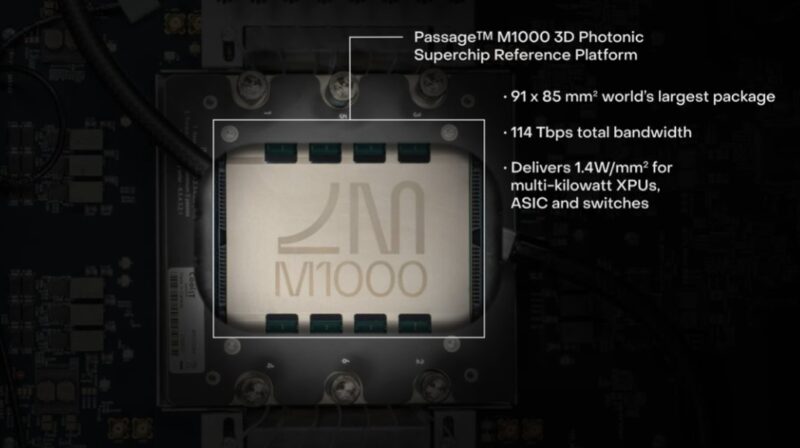
With all of this, the Passage M1000 offers 114Tbps of bandwidth.
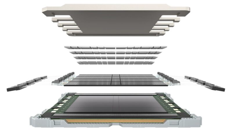
Here is a CAD view of the chip that we found.
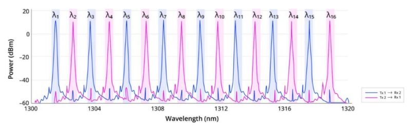
Here is a quick visual on what is meant by lambdas and having sixteen peaks and valleys for signaling across different wavelengths.
The real benefit here is being able to increase density by increasing the utilization of each connected fiber, sending more signals over the same strand. More throughput per fiber strand means that future (much larger) AI accelerators can push more data from a given area to the network.
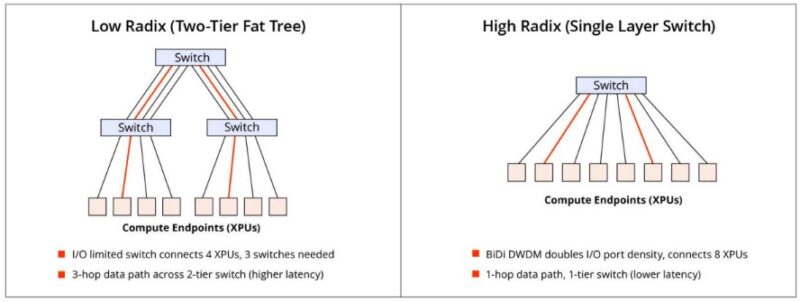
Lightmatter also shows this as a savings on switching and network radix. The above diagram is a small scale, but imagine that with millions of XPUs. The network side is actually one of the big scaling challenges in large AI clusters.
Final Words
DWDM is not a new technology itself. I remember my father talking about this almost 30 years ago in the late 1990s. The big innovation here is using it in co-packaged optics to increase the bandwidth available to future XPUs. One of the challenges of this technology is that as you pack signals into a tighter range of wavelengths, the tolerance for things like heat expanding channels and shifting wavelengths is real. Lightmatter has to overcome these physical challenges in its solution, which is why a big test chip like this is also important.


So that’s the M1000 chip with the funny “LM” logo on it. I found a photo of this chip by chance in a randon search for chip pictures. This article explains what I found. Thanks, Patrick.
The big deal here is having 16 lambdas in non-PM (polarization-maintaining) SM fiber which is more expensive and has higher attenuation than “normal” SM fiber.
Lightmatter has indeed overcome the kinds of thermal challenges alluded to in this last paragraph of this article. We’ve captured it on video: https://lightmatter.co/resource/lightmatters-8x-leap-world-first-16-wavelength-bidirectional-optical-link-for-ai-data-centers/
The article is not very clear, but this solution is an interposer that can be used to build accelerators that use optical communications instead of electrical signals.