
In this piece, we are going to go a bit deeper in the microarchitecture features of the new Intel Xeon Scalable Processor Family. We are doing extensive coverage of the Intel Xeon Scalable Processor Family Launch including platform level, chipsets, mesh interconnects, benchmarks, vendor launches, and SKU stacks. Check out our Intel Xeon Scalable Processor Family Launch Coverage Central for more information. Since the new processors are a huge piece of text to keep writing out, you may see us use the official codename of Skylake-SP in this article.
We are going to focus this piece specifically on Skylake core architecture and one of the major new instructions, AVX-512.
Starting with a Skylake Core
We start the microarchitecture discussion with the basic Skylake-SP core. What may surprise some readers is that this is essentially a basic Skylake core that we have seen Intel use for years, and then add additional L2 cache and an additional FMA and AVX execution unit bolted on.
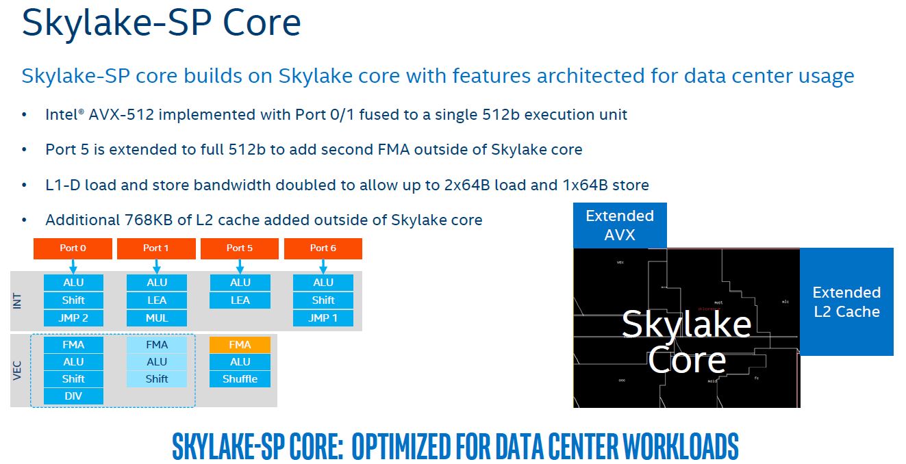
Not all chips will have the second FMA unit. That is another part of the differentiation between the various processor tiers.
Here is the slide that describes some of the more technical microarchitecture improvements over Broadwell-EP.
The net impact is that Intel expects a roughly 10% IPC improvement over Intel Xeon E5-2600 V4 cores (Broadwell-EP.) Our later benchmarking will show that at the same clock speed, we expect a >30% performance per clock improvement over Intel Xeon E5-2600 V1 cores (Sandy Bridge-EP.)
That is an important metric for two reasons. First, Intel Xeon E5-2600 V1 servers are those that will be hitting a 5-year refresh cycle with the Intel Xeon Scalable Processor Family generation. Second, that 30%+ IPC improvement is combined with a maximum core count increasing from 8 to 28 cores. This is the replacement cycle where consolidation can happen at an enormous scale. A general rule of thumb is that at the same clock speeds a three Skylake-SP chip will perform about equal to four Intel Xeon E5-2600 V1 cores.
Major Intel Xeon Scalable Processor Family L2 and L3 Cache Changes
If you compare the Skylake-SP core to a desktop Skylake core, you will notice that the L2 cache is much larger than the desktop counterpart. The server part has an additional 768KB of L2 cache for a total of 1MB L2 cache. Intel made this change in order to increase the amount of low latency data it has available to each core.
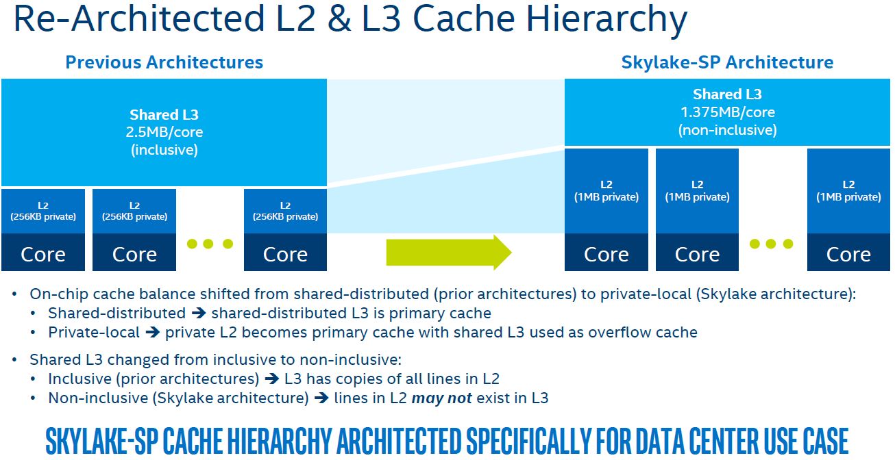
At the same time, Intel reduced the L3 cache by almost half from 2.5MB/core in Broadwell-EP to 1.375MB/core in Skylake-SP. That reduction helps Intel with transistor budget to increase the L2 cache size and core counts all on a 14nm process.
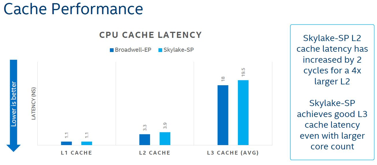
The question of why Intel would do this lies in cache latency. L2 cache is 3.5-4x faster than L3 cache. As core counts rise, L3 cache latencies rise so Intel needs to move more data closer to the CPU.
One methodology Intel is using is to make the L3 cache non-inclusive. Here is Intel’s slide describing the difference and the process:
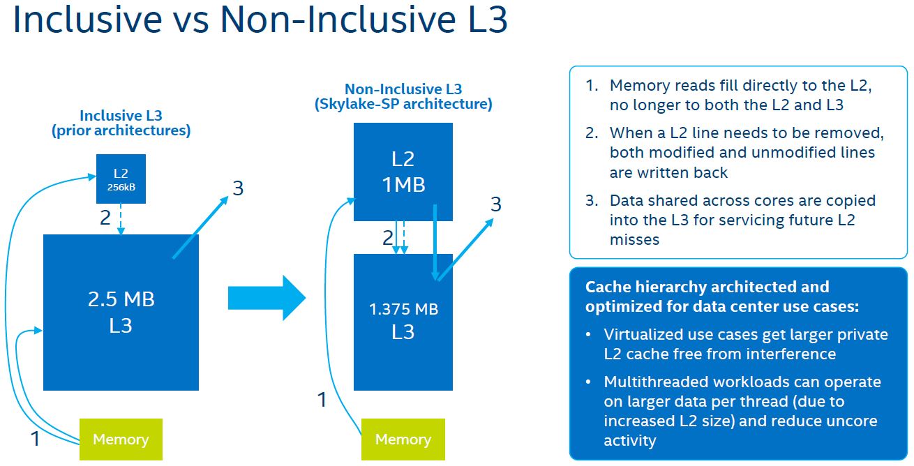
The key here is that instead of data being copied both to L2 and L3 caches, data can be loaded directly into the L2 cache. If you are a storage professional accustomed to storage tiering, this is roughly similar to being able to load data directly to an NVMe tier and then working with it and then pushing data, as it is less frequently used to a SATA/ SAS SSD tier or HDD tier instead of needing to copy it to both tiers before using it.
To be clear, the total cache size goes down with this design. L2+L3 on Broadwell-EP was 2.75MB while on Skylake-SP it is 2.375MB. The Broadwell-EP L3 cache has a copy of the L2 cache data so effectively it is a 2.5MB total cache.
Intel never gave us this view, but through a long presentation, but the extremely rough sketch of why this works looks something like this:
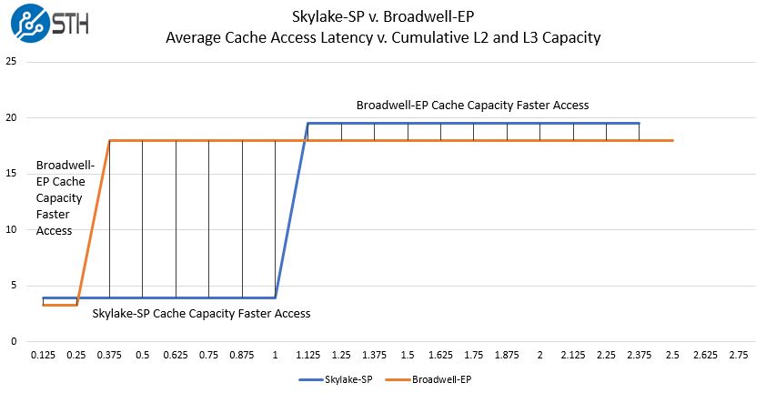
Effectively since each core is able to get more low latency L2 cache, it can get big gains at capacities between 256KB and 1MB while giving up relatively little from 0-256KB and 1MB to 2.375MB. The final 128KB is the remaining delta in effective cache sizes.
That is a very rough diagram to illustrate the trade-off. The obvious other factor is that the shared L3 cache means that the higher latency data in Broadwell-EP’s L3 caches are available to other cores. With Skylake-SP there is not as much of this shared L3 cache data on the chip.
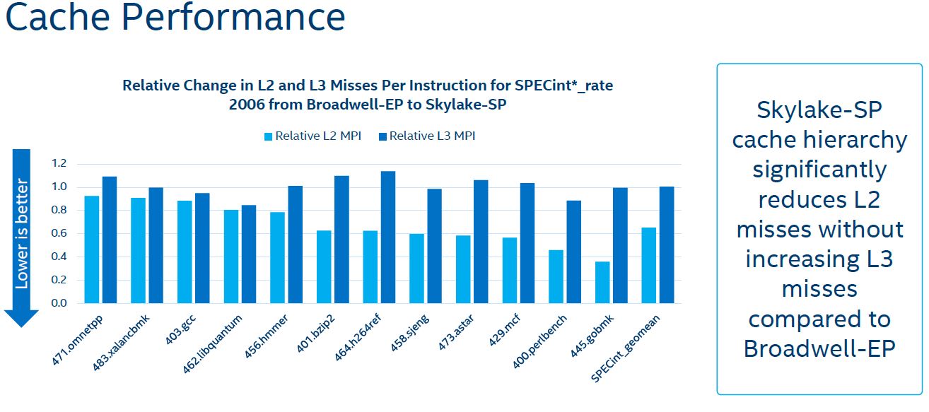
In practice, this means that combined with the Skylake-SP mesh improvements, most of the time Skylake-SP is faster, while sometimes Broadwell-EP is faster. Here is Intel’s data using SPECint_rate 2006 components:
Here is the SPECfp_rate 2006 version of that chart:
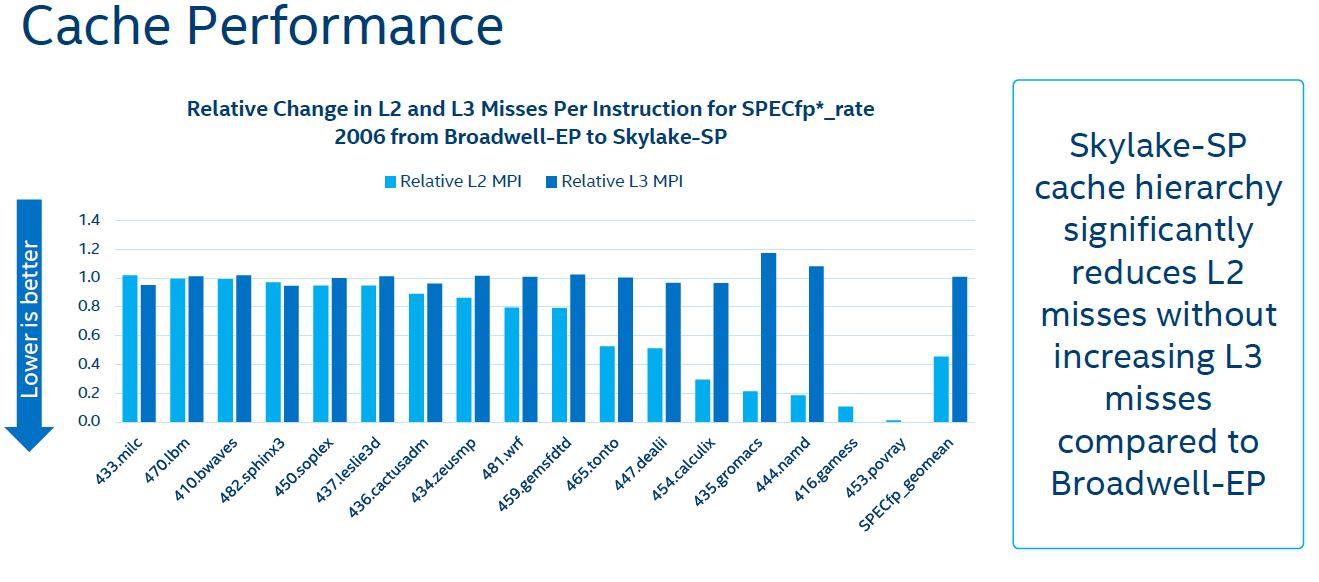
Essentially what this data is telling us is that for SPECint and SPECfp workloads, having a larger L2 cache means that the probability of hitting low latency caches go up. It also tells us that for these workloads L3 cache misses are relatively similar even with the smaller inclusive L3 cache of Skylake-SP.


“Intel Xeon Phi may be on the road to an untimely phase out.”
It does leave Xeon Phi in bit of a pickle. However, all is not lost.
First, the MCDRAM advantage means most applications that are bound by memory bandwidth will have an advantage to the Xeon Phi. A not insignificant number I hear.
Second, the peak Flops is still noticeably higher on the Phi. The 8180 with 2.5GHz AVX-512 frequency would have 2.2TFlops of performance. Xeon Phi 7250 has 2.6TFlops and 7290 has 3TFlops.
In DL workloads we’ll see Knights Mill in a quarter or so. While the DP performance is said to be somewhat reduced, you get Quad Vector extensions for 32-bit to double SP FP performance and also half-precision vector support for yet another 2x increase in DL performance for a total of 4x. That would result in 6-7TFlops in SP FP and 12-14TFlops in 16-bit FP.
The real threat is Nvidia. Volta is already out and beats Knights Mill in SP and 16-bit FP a bit, trounces it in DP FP, and crushes it on Tensor flops.
Xeon Phi also has second OmniPath connections for better scaling on mass scale.
Comments are closed.