
This week we covered the Intel Foundry event and some of the new innovations in both fabrication and packaging technologies coming. Something we also wanted to cover is the innovation that Intel pre-announced for its Clearwater Forest line. This is set to be a high-core count game-changing server CPU with multiple technological breakthroughs. Let us get to why.
Intel Clearwater Forest is Set to be a Tech Breakthrough Server Chip
A quick level set for those who do not follow code names. Sierra Forest is the all-E-core Xeon scaling up to 288 cores in some versions that will launch this year. Our chief Patrick might be the most excited person on the planet for this as he tells our team, and others about it all the time. The idea is to pack a ton of energy-efficient cores, without the side-channel impacts of Hyper-Threading, into a dense CPU package. We are going to see 500+ cores per U in blade systems later in 2024.
Sierra Forest, as cool as it might be, is still a first-generation product. Many customers are looking ahead to Clearwater Forest. Clearwater Forest is currently set to be the leading Intel 18A Xeon processor incorporating that node’s set of technologies as well as advanced packaging. Another way of saying it, we expect more cores with more performance and better power efficiency.
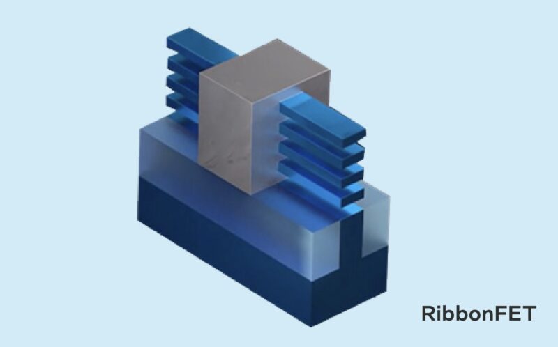
The first big technology is the 18A process technology. That means that we get RibbonFET replacing the FinFET technology that has been used for about a decade and a half.
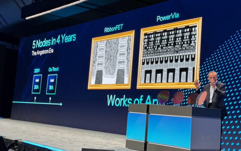
RibbonFET has the transistor gate wrapped around the channel, and these can also be made in different widths. The result is a more efficient transistor.
The second big technology is the PowerVIA. Intel is delivering backside power which we heard multiple folks at the Foundry event this week say they expect about 6% improvements just from that alone.
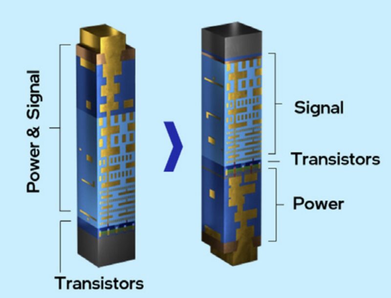
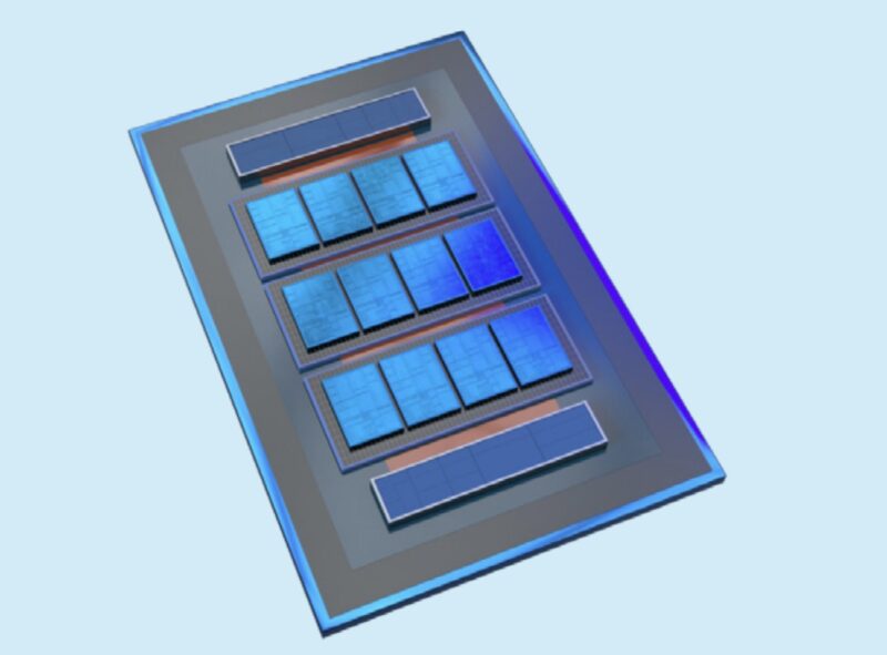
On the packaging side, for Clearwater Forest, Intel says that it is going to use other process nodes for SRAM and I/O that do not scale as well on newer processes. AMD has its IO Die introduced with the EPYC 7002 series “Rome” on a different process for I/O. AMD also has 3D V-Cache we first reviewed with Milan-X and then Genoa-X. Our guess is that AMD is going to have to introduce a similar cache technology for future cloud-native CPU versions because everyone in the industry is running into the reality that SRAM is not scaling. Intel’s version, however, appears to put dies with cores atop cache dies.
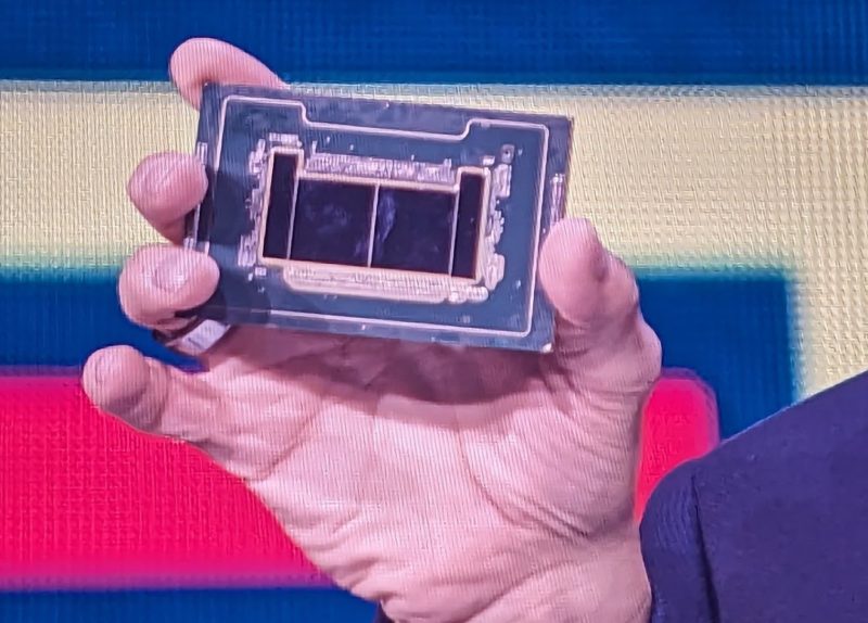
Intel is planning to use Foveros Direct 3D which involves direct die-to-die copper bonding between top tiles and base dies. When we look at the pictures of Clearwater Forest above, we can see the compute dies on what are likely SRAM and fabric base dies.
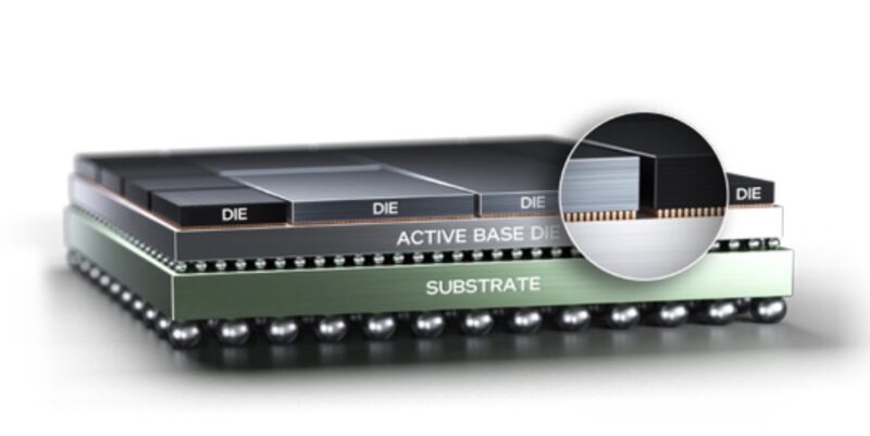
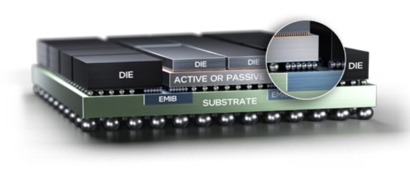
Another packaging technology coming on Clearwater Forest is Intel EMIB 3.5D. Here, Intel is combining several of its technologies like its EMIB (chip-to-chip bridge) and Foveros Direct 3D is called EMIB 3.5D.
New process and new packaging make Clearwater Forest exciting from a technology point of view.
Final Words
For folks new to the server industry, may not remember the day when Intel had process leadership over TSMC. Clearwater Forest if delivered on time with 18A is going to be very powerful. Huge numbers of E-cores, allowances for bigger caches, and more I/O have the opportunity to change the game compared to Q1 2024 Xeons. By 2025 (if schedules hold), we are going to look back at today’s chips and think they are ultra low core count, power-hungry parts. We are a far way from just a process shrink with a few more cores being added.


What is Intel 18A exactly? 5nm + 7nm for IO die?
> Sierra Forest is the all-E-core
thats sad. i wonder if AVX512 is gone for good in server space.
18A is 18 angstroms, it’s similar to TSMCs upcoming 2nm process. The compute chiplets for clearwater forest will be made with the 1.8nm processes, the base die with a 4nm process and the IO die with a 7nm process.
Intel will still have all P-core counterparts in the same socket with granite rapids and then diamond rapids. Intel will have moved beyond AVX512 by then anyways; with AVX10.2 E-cores will have 512-bit FP/Int pipelines.
@Paul: AVX10 version does not dictate the width of execution, both 256- and 512-bit are going to be supported from AVX10.1. We have no indication that E-cores will ever support 512-bit.
Unfortunately this distinction is not automatic and software compiled for 256-bit version will not be able to switch to 512-bit width automatically like ARM SVE is capable of. Either recompilation or mechanisms like dynamic dispatch will have to be used to maximize usage, just like with AVX-512 currently. However P-cores might be able to still run the 256-bit version faster due to more execution units. Of course they will also have more cache, higher frequencies and newer microarchitecture in general.
This is still a benefit for E-cores because AVX10 brings a lot of features from AVX-512, regardless of 512-bit width.
Wake me up when it’s actually for sale. Otherwise think I’ll sit this unfounded hypetrain out. After all, the last time we got to hear about the tech that was the stuff of the future of humanity we got Sapphire Rapids. Late. Late some more. Then more lateness. Followed by underwhelming everything. But sure, let’s pretend the company that has spent the last 4-5 years chopping and selling parts of itself off, flopping around pulling its old, “here’s our new gen, same as the old gen,” routine, and generally putting more talk out there than product that resembles what those words claim will magically be able to swap production methods, put together the next great chip, and then combine those two things.
Granite Rapids’ CXL 2.0, per core AMX accelerators and 8800MT/s memory upgrade, will be plenty to talk about in 2024.
Who remembers a time Intel delivered on their promises? Yeah, me neither…
Intel and not delivering on promises are practically a synonym nowadays
Or a iconic duo. Maybe both!
“thats sad. i wonder if AVX512 is gone for good in server space.”
No. Quite alive and well in the P Core versions. This does not need or benefit from AVX.
“Who remembers a time Intel delivered on their promises? Yeah, me neither…”
Short memory. Since Ice Lake there has been a yearly cadence of releases.
“Intel and not delivering on promises are practically a synonym nowadays
Or a iconic duo. Maybe both!”
AMD fanboy. Intel has delivered on everything it has promised.
“Wake me up when it’s actually for sale. Otherwise think I’ll sit this unfounded hypetrain out. After all, the last time we got to hear about the tech that was the stuff of the future of humanity we got Sapphire Rapids. Late. Late some more. Then more lateness. Followed by underwhelming everything. But sure, let’s pretend the company that has spent the last 4-5 years chopping and selling parts of itself off, flopping around pulling its old, “here’s our new gen, same as the old gen,” routine, and generally putting more talk out there than product that resembles what those words claim will magically be able to swap production methods, put together the next great chip, and then combine those two things.”
He cut the fat and cut the divisions that had accumulated.
You don’t understand business or tech – typical for an AMD Fanboy.
Run along
Given their approach with multiple tiles I believe they still have yield issues bringing up pvia and RibbonFET at 18A together.
MB007 –
Sorry wrong – Intel has always been the yield kings. Going back to Xeon Scalable Gen 1 – the cut down cores (28C in a perfect die) were virtually unavailable since the yields were so high.
Same with Ice Lake.
Yield is not an Intel issue – the reason AMD used their “chiplets” was because TSMC could not create larger die without defects – and AMD was basically bankrupt and wanted to use every possible sliver of silicon…
You believe? Based on what? Your fee fees?
Intel has been using MCM for quite some time – even in 1995 with the Pentium Pro – MCM.
Sorry but you are just trying to make TSMCs atrocious yields onto Intel.
LOL shit only intel fanboys say
…who got his SPEC results deleted, because he lied?…
Please leave all the fanboie accusations at WCCF. This is a grownups site.
Some hours after my above post yesterday (3:05 pm) with
“…who got his SPEC results deleted, because he lied?…”
I wrote you, that I want to correct my post, but whyever, you did not publish it. Perhaps because it linked to another website.
As I saved my post via screenshot I want to re-send it here, and you might leave the link out and somebody can find infos to this SPEC thing from Intel on your sites, as I later saw. My post was:
##begin##
I wrote “…who got his SPEC results deleted, because he lied?…”. I want to correct:
“SPEC has effectively invalidated more than two thousand SPEC CPU 2017 benchmark submissions after it was discovered the Intel oneAPI DPC++ compiler was effectively “cheating” per their standards with a targeted optimization.” as can be read here:
https://www.phoronix.com/news/oneAPI-DPC-Compiler-Cheat-SPEC
##End##
And there it is, delayed again a full year into 1H26, likely will end up as a 2H26 product anyway, and thus swiftly swing into actually be a 2027 product.
Comments are closed.