IBM Nanostack: Transistors Grow Up By Going Up
So what will follow GAAFET/nanosheet transistors then? For several years now, Imec and other research organizations have been proposing the complementary FET, or CFET. There are multiple specific implementation ideas for CFETs, but the brief version is that CFETs will pick up the torch by building transistors on top of each other. Rather than trying to shrink transistors in planar (xy) dimension any further, resulting in parts too small to reliably contain electrons, transistors would be built in the third dimension as well, stacking materials on top of materials in order to contain the flow of electrons. The idea of 3D stacking transistors has been proposed for many years now – and we even have forms of it in memory technologies such as 3D layered NAND – but the complexity of building transistors in this fashion has always been immense.
None the less, as GAAFETs run out of headroom, more complex technologies become necessary, and this is when 3D stacked transistors are expected to become necessary to keep Moore’s Law moving along.
To that end, IBM Research has developed a design for stacked transistors which they are calling Nanostack. After a run through industry and academia with papers published at VLSI 2026 and elsewhere, the company is preparing to bring greater public attention to the technology by briefing the press and the rest of the wider world on the technology. IBM Research hopes for the technology to become the foundational design of next-generation transistors, while IBM’s corporate office hopes to be able to license the technology out to chip fabs as the basis for their respective post-GAAFET technologies.
In regards to design, while IBM’s announcement is very careful to never use the term CFET (and the company declined to address the matter in a press Q&A), the overall design of their nanostack architecture is relatively similar to what Imec has proposed as the sequential CFET.
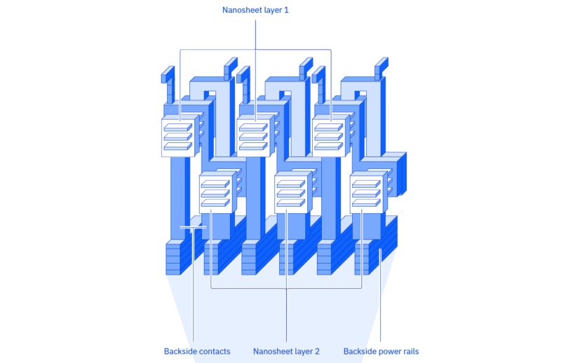
In the IBM nanostack design, the company is essentially forming a CMOS transistor by stacking two smaller GAAFET transistors on top of each other. Specifically, the company’s design involves building an nFET transistor and then stacking the complementary pFET transistor in a staggered fashion on top of it. Each of these transistors would be comprised of multiple layers of nanosheets, analogous to today’s GAAFET nanosheet transistors, giving rise to the nanostack name.
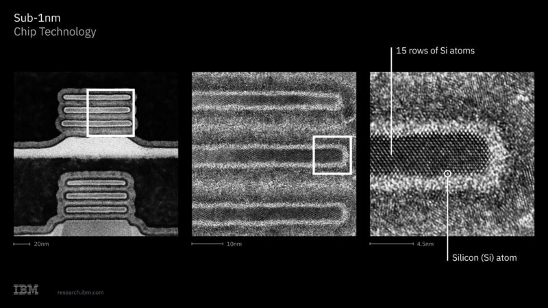
The resulting transistors are, in turn, able to be incredibly small. While IBM is not sharing any deep (and comparable) details at this time such as gate pitches or metal pitches, the nanosheets themselves are only 15 silicon atoms thick. And the distance between the sheets is only a big bigger, at around 9nm or 27 atoms. Modern silicon lithography has often been lightheartedly referred to as atomic printing, and at these scales, the nanostack is not too far off from that.
Of the key manufacturing innovations needed to make this possible, by far the biggest step is direct wafer-to-wafer bonding. Because the pFET and nFET transistors are made on different wafers, aligning them is not just a matter of slowly building a transistor on a single wafer, but now the process must be done twice and then the transistors aligned on an atomic scale. Wafer bonding is already being used in products such as MEMS chips, but what IBM is intent on doing requires an even greater level of precision, control, as well as novel means of bonding the wafers together.
Actually accomplishing this gets in to a level of materials science that IBM is not going into at this time, but the high-level overview is that they are using an ultra-thin dielectric to bond the transistors together. Specifically, IBM is using a material that is robust enough to provide a solid connection between the FETs, but is thin enough to keep its capacitance at a minimum in order to make the stacked transistor viable.
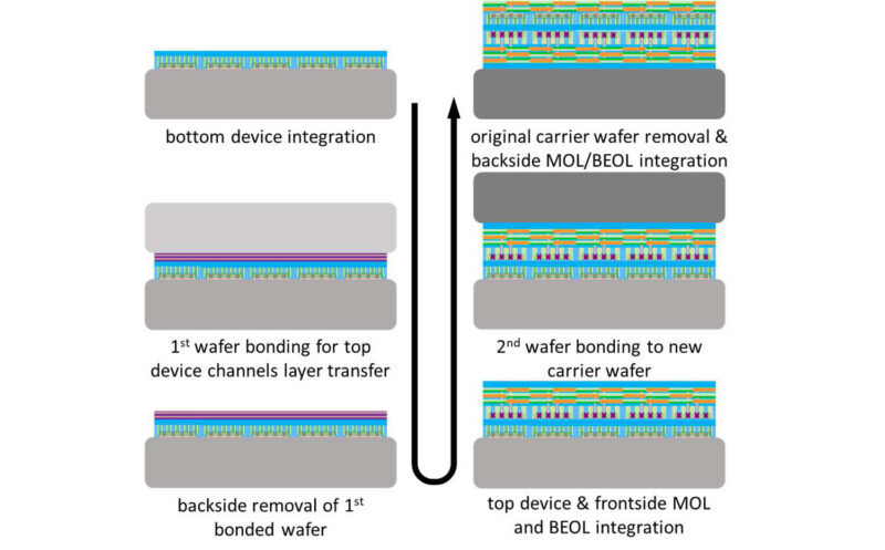
Speaking of materials science, that the nanostacking process uses multiple wafers is another aspect that IBM considers to be a significant benefit. Producing pFET and nFET transistors on separate wafers means that the materials used in each wafer can be optimized for their respective transistor type, as well as their role as the top or bottom half of the transistor. What these materials are IBM will not say (and at 5+ years out, they likely have not finalized their choices), but it is a major differentiator from GAAFET and previous transistor designs, where the material choices were limited to whatever worked on a single wafer. The fact that only half a transistor is being fabbed on each wafer is also being touted as a benefit in the manufacturing process, since it means that the fabbing process for each wafer can be simpler than contemporary monolithic transistors.
Finally, it should be noted that besides literally building chips by placing wafers on top of each other, IBM’s nanostack efforts are also building on top of other innovations that the company and other researchers and fabs have commercialized or are in the process of doing so. Backside power delivery networks are mandatory for nanostacking to work (both sides of the bonded wafers are the backside), and that technology is just now coming to market in nodes like Intel’s 18A. High-NA EUV will be another critical component, and along with being a research subject for IBM, the company’s research division is also set to receive one of ASML’s high-NA scanners in order to help refine the manufacturing process for commercialization. The net sum being that a number of additional technologies are first needed to pave the way for nanostacking.
Nanostack Benefits: 50% Smaller with 50% More Performance or 70% Lower Power
So what would nanostack transistors entail for full chips, then? Compared to IBM’s 2nm GAAFET transistor technology, the company expects nanostack transistors to be roughly 50% smaller – effectively doubling transistor densities over their 2nm process. At this point IBM is not disclosing specific density figures (and this depends on what type of circuit is being fabbed, among other things), but 2nm-era GAAFET processes roughly range from 230 million to 310 million transistors per mm2. So for IBM to double that would lead to chips with transistors densities near or north of 450 million per mm2. Or, as IBM likes to put it, on the order of 100 billion transistors in an area the size of a fingernail.
Of particular interest here is that IBM’s research has shown that these kind of area scaling gains are not limited to just logic gates. The company’s research team has also demonstrated that they can achieve a 40% reduction in SRAM cell size as well, which would be a significant improvement in a circuit type where gains are even harder to come by. While the final generations of FinFET technology have continued to reduce logic size, the same has not been true for SRAM cell size, and as a result chip designers have not been able to scale up the amount of SRAM in their chips as quickly as they have been able to scale up the number of logic gates. Consequently, being able to deliver significant improvements in SRAM cell sizes would be incredibly welcome – and especially as SRAM is now coming back into focus as a key component for high-performance AI accelerators.
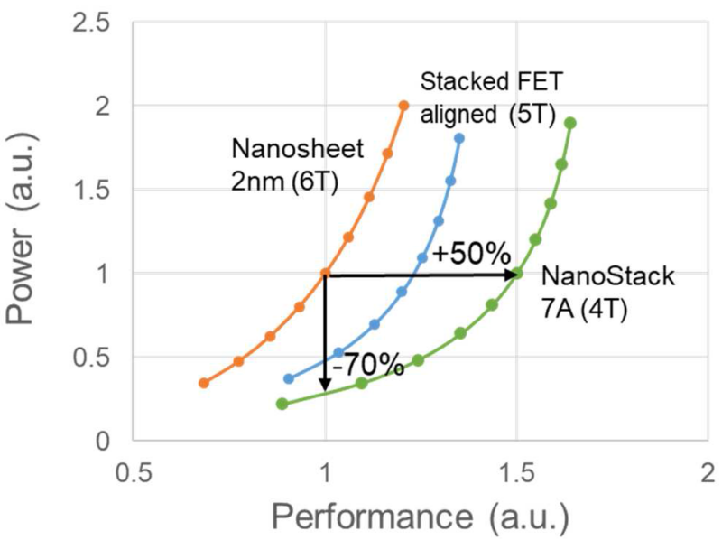
As for logic gate performance, IBM is touting nanostack transistors as being able to offer capabilities ranging from a 50% increase in performance at iso-power, or a 70% decrease in power consumption at iso-performance compared to their 2nm node. The specific benefits will depend on the type of circuit built and what parameters a chip designer and fab decide to optimize for, but compared to 2nm it leaves chipmakers with a wide range of options. However, like other recent process node innovations it is an either/or situation: chipmakers can have 50% more performance or 70% less power, but not both at once. In practice, most will likely choose a point between the two, but it means even with nanostack transistors the industry is well past the days of being able to get major improvements in both power and performance with a single node.
It is also worth keeping in mind that IBM’s figures are comparing things to their 2nm node, which is their first-generation GAAFET node. GAAFET is expected to be around for multiple process nodes, each of which are slated to deliver modest improvements to size and performance characteristics, so while IBM’s nanostacks are predicted to be a massive leap from first-generation GAAFET, they likely are not going to be as great of a leap compared to the last generations of GAAFET.
Speaking of production, IBM is aiming for a rather aggressive production timeline for chips based on nanostack transistors. The company believes that the technology can be ready in time for 7 angstrom (0.7nm) chips, which would have nanostacks in commercial production in as little as 5 years. From IBM’s perspective they have solved the question of whether it is even possible to build a nanostack transistor (they have) and now it is merely a question of refining it and scaling it up for mass production.
As an aside, the 7 angstrom target should not be considered a comment on the size of nanostack transistors, either. As IBM was quick to remind the press, node names have no real bearing on the size of a transistor these days – and it has not for quite some time.


