
AMD is presenting its Versal RF Series at Hot Chips 2026. This adaptive SoC family targets wideband RF signal processing across defense, test and measurement, communications, and quantum control. We do not cover this as much, but here we go.
We are covering this session live, so please excuse typos.
AMD Versal RF Series at Hot Chips 2026
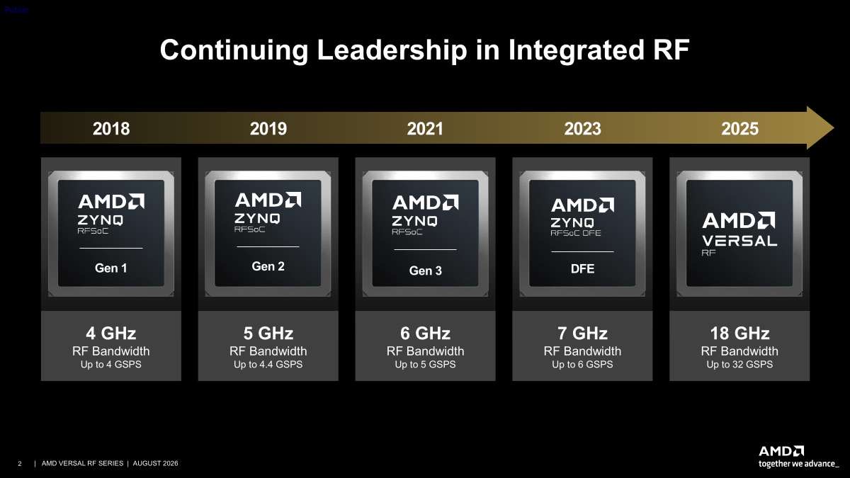
AMD’s integrated RF timeline runs from the Gen 1 RFSoC parts of 2018 through the 2023 DFE family, with RF bandwidth climbing from 4 GHz to 7 GHz along the way. Versal RF Series represents the huge Zynq to Versal 2025 jump
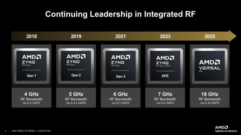
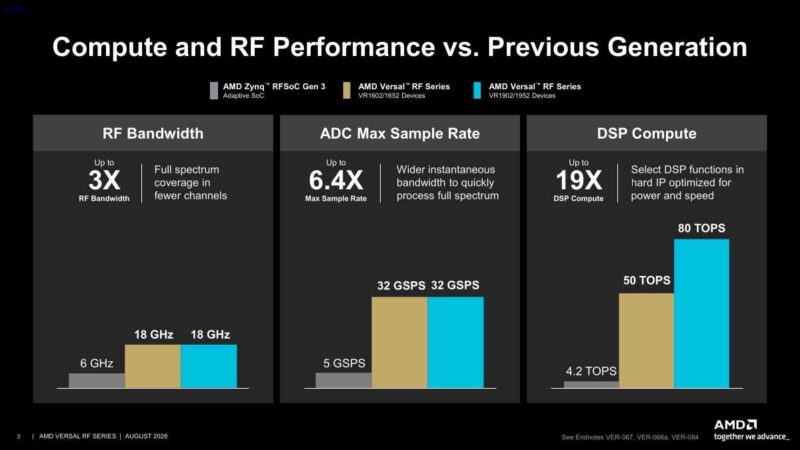
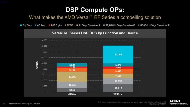
AMD claims up to 19x the DSP compute and 6.4x the maximum sample rate, with the new parts reaching 32 GSPS on the ADC side and 18 GHz of RF bandwidth compared with 5 GSPS and 6 GHz on Gen 3. This family tops out near 80 TOPS of effective DSP compute.
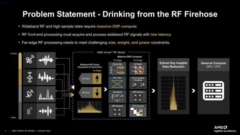
A wideband front end moves enormous amounts of data, so the real work is collapsing that stream into useful intelligence at the far edge while meeting size, weight, and power limits. This signal chain runs from the RF-ADC through a first-stage channelizer into the AI Engine array, then a second-stage channelizer and general compute, bringing an 18 GHz input down toward 1 MHz for analysis.
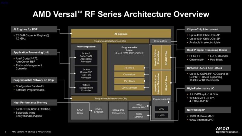
This architecture overview pulls together hard IP, a processing system, and the AI Engine array. Two Arm Cortex-A72 cores and a pair of Cortex-R5F processors handle control, while hard FFT/iFFT, channelizer, LDPC decoder, and poly block units offload the bandwidth-heavy DSP. RF-ADCs reach 32 GSPS and RF-DACs 16 GSPS across 18 GHz of RF bandwidth, with DDR5 and LPDDR5X memory plus UCIe chip-to-chip links in the mix. If you just read our AMD Versal Premium Gen2 coverage at Hot Chips 2026, this is the slide I was hoping to see in that presentation (albeit for a different part!)
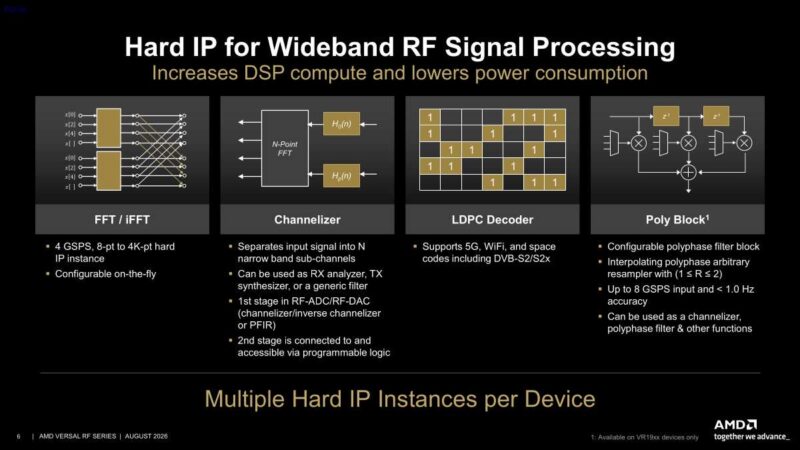
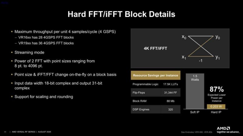
AMD also moved a lot of memory on-chip, continuing the Versal trend we covered when the company shifted Memory-on-Package from HBM to LPDDR5X. Hard IP is the mechanism that turns raw bandwidth into tractable compute. These FFT/iFFT blocks run at up to 4 GSPS with point sizes from 8 to 4096, and the channelizer splits a wide input into N narrow sub-channels at up to 8 GSPS. Putting these functions in hard blocks increases DSP compute while lowering power compared to soft programmable logic.
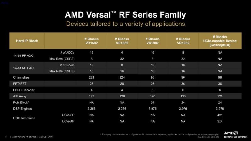
Versal RF Series ships as four near-term devices plus a UCIe-capable part. VR1602 and VR1652 carry the wideband flavor, with VR1602 at 16 eight-GSPS ADCs and VR1652 switching to four 32-GSPS ADCs for the highest sampling on a single die. VR1902 and VR1952 add more DSP engines plus a poly block for extra flexibility, while the whole family leans on 14-bit converters.
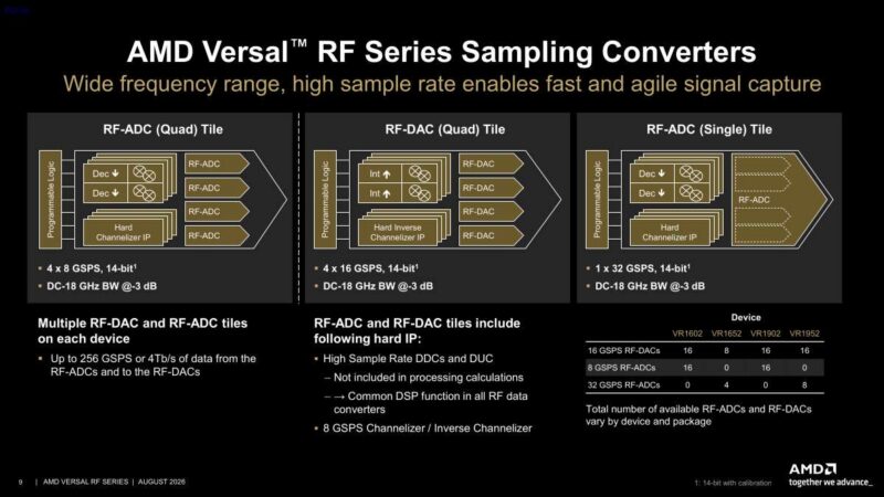
These converter tiles are where the wideband story starts. An RF-ADC quad tile delivers 4 x 8 GSPS at 14-bit, an RF-DAC quad tile runs 4 x 16 GSPS, and a single ADC tile reaches 32 GSPS, all with DC-to-18 GHz bandwidth. AMD points to up to 256 GSPS, the equivalent of 4 Tb/s, of aggregate data moving from the ADCs into the on-chip DSP.
AMD breaks operations by function and device for the VR16xx and VR19xx families, with the peak channelizer case landing around 31,104 GOPS of total DSP throughput. Often compute comes from hard IP rather than the fabric, which is why these Versal parts are perhaps not considered “just” FPGAs at this point.
Each hard FFT/iFFT block sustains 4 GSPS in streaming mode. VR16xx carries 28 of these blocks and VR19xx 36, spanning power-of-two point sizes from 8 to 4096 with point size and FFT direction switchable on the fly. AMD estimates a hard block uses about 87 percent lower power than the equivalent soft implementation.
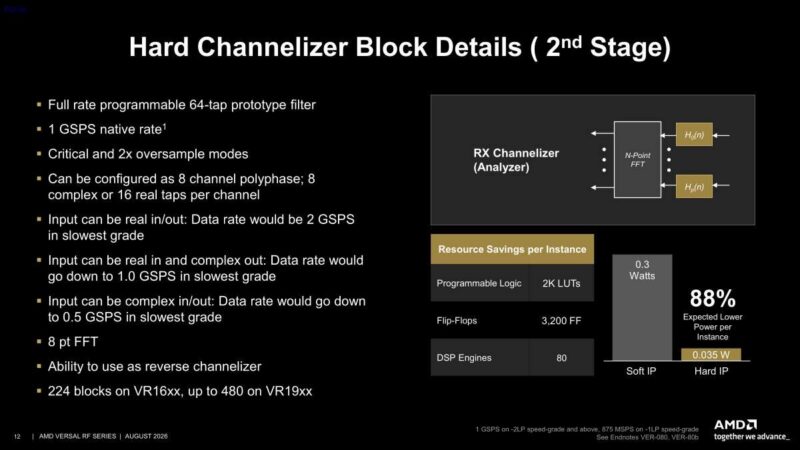
This second-stage channelizer is the follow-on filter bank. Each block runs a 64-tap prototype filter at a 1 GSPS native rate and can be configured as an eight-channel polyphase filter with complex or real taps. Versal RF puts 224 of these on the VR16xx and up to 480 on the VR19xx at just 0.035 W per instance.
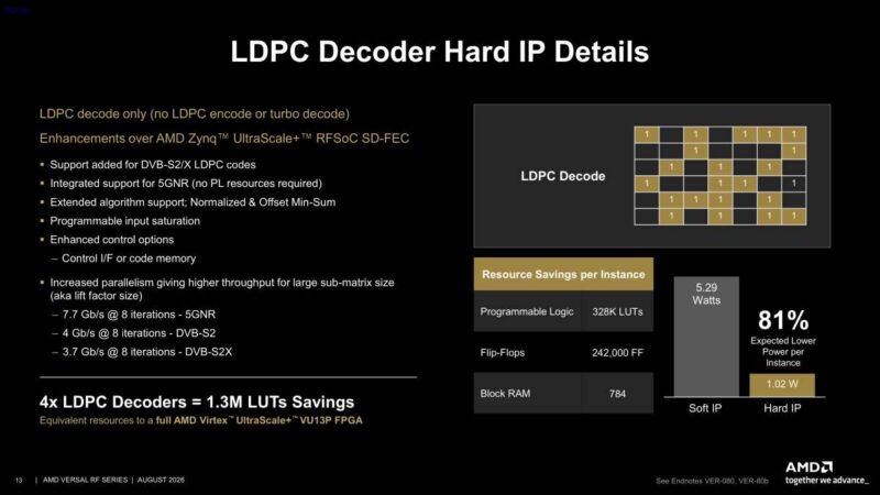
This LDPC decoder hard IP targets 5G and satellite links. This block sustains 7.7 Gb/s at eight iterations for 5G NR, 4 Gb/s for DVB-S2, and 3.7 Gb/s for DVB-S2X, with 5G NR support requiring no programmable logic resources. AMD frames four of these decoders as equivalent to a full Virtex UltraScale+VU13P FPGA.
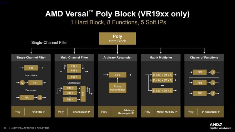
This poly block is exclusive to the VR19xx parts. One hard block folds in eight functions, from single- and multi-channel FIR filters to an arbitrary resampler and matrix multiplier, exposed through five soft IP layers. That makes it a flexible building block for resampling and channelization schemes.
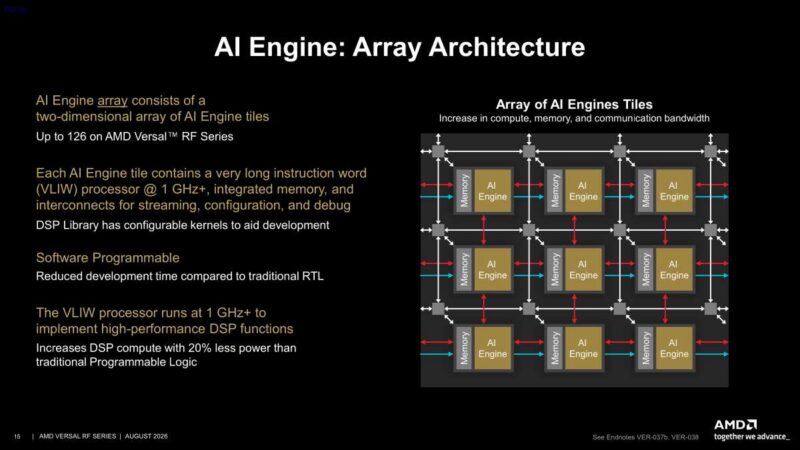
This AI Engine array is the programmable workhorse for the DSP. There are up to 126 tiles, each packing a VLIW processor running over 1 GHz plus integrated memory, to handle the wideband processing. AMD says the array delivers about 20 percent lower power than the equivalent programmable logic.
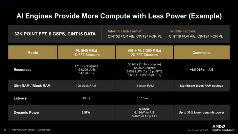
For a 32K-point FFT at 8 GSPS, running the math on AI Engines plus programmable logic cuts LUT use from more than 153,000 down to about 8,000, drops latency from 48 microseconds to 7.5, and uses up to 30 percent lower dynamic power versus a programmable-logic-only structure.
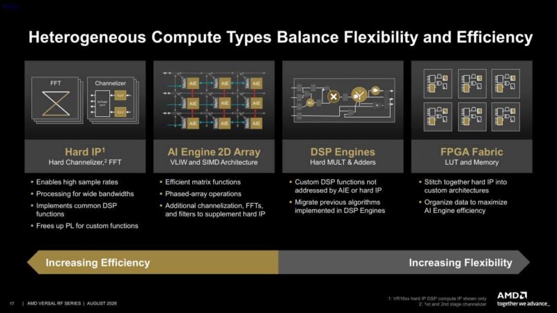
This device balances four compute types, each trading efficiency for flexibility. Hard IP and the DSP engines handle the highest sample rates and common DSP functions. The AI Engine array performs wideband processing. Fabric stitches everything into custom architectures. AMD is framing this as putting hard IP where efficiency matters and fabric where flexibility does.
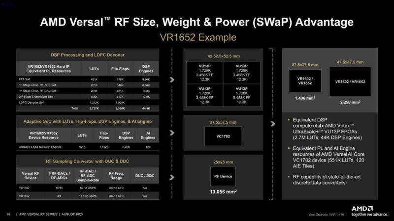
Size, weight, and power are a central selling point at the far edge. AMD says a single VR1602 or VR1652 delivers the equivalent DSP compute of four Virtex UltraScale+ VU13P FPGAs, along with the programmable logic and AI Engine resources of a Versal AI Core VC1702, in a 37.5 x 37.5 mm package. Consolidating all that silicon into a single adaptive SoC is the entire point for constrained platforms.
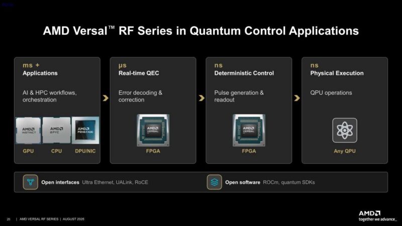
Quantum control is one of the more novel target applications we have seen in Hot Chips presentations. AMD is mapping the latency hierarchy of quantum systems, from error decoding and correction at millisecond timescales to pulse generation and readout at nanosecond timescales. Versal RF sits between the host GPU and CPU compute stack and the QPU.
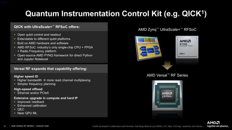
This Quantum Instrumentation Control Kit builds on AMD’s RFSoC. QICK, developed with Fermilab, Oak Ridge National Lab, and the Department of Energy, uses the single-chip CPU plus FPGA plus radio platform for open qubit control and readout. Versal RF extends that with higher bandwidth for more read channel multiplexing, simpler frequency planning, and high-speed Ethernet or PCIe Gen5 offload.
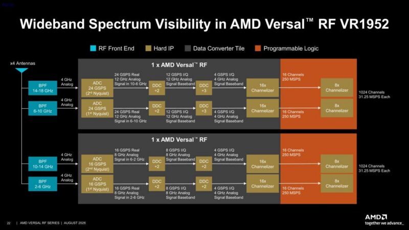
This VR1952 figure shows several independent wideband receive paths running off a single device. Each antenna feed spans a 4 GHz slice, so a handful of feeds cover roughly 2 to 18 GHz, with deep channelization keeping individual sub-channels down around 31.25 MSPS. That gives operators continuous spectrum visibility across the whole band rather than a narrow-tuned window.
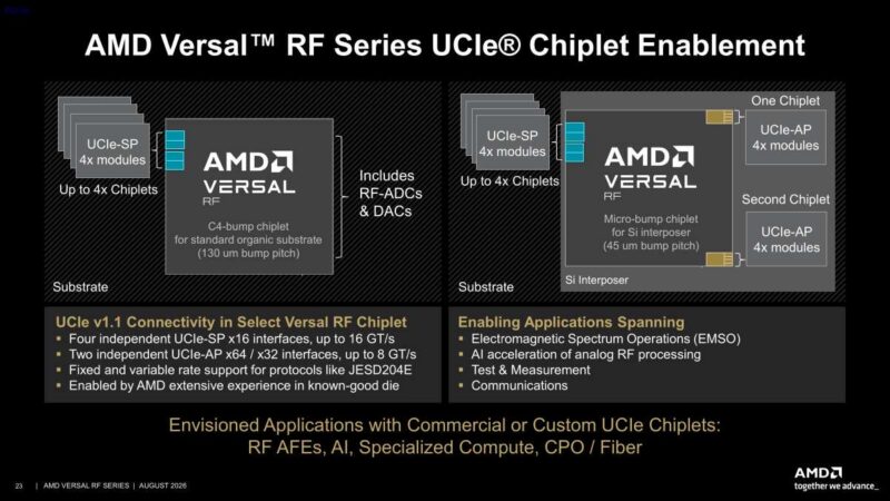
UCIe chiplet support opens an expansion path for the family. This device exposes UCIe-SP x16 interfaces at up to 16 GT/s and UCIe-AP x64 or x32 links, letting designers attach up to four chiplets over a silicon interposer. AMD sees commercial or custom chiplets for RF front ends, AI, and specialized compute. This broader UCIe interconnect standard is worth a look for how these links fit together.
Here is the summary slide.
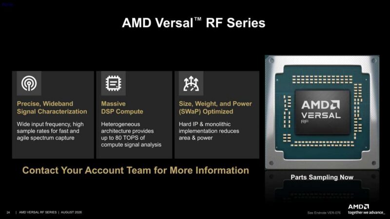
Since I am falling behind, I will let you read this one.
Final Words
To me, this is neat because it feels like a concrete example of what I remember Victor describing as Xilinx’s vision when Xilinx launched the Versal family many years ago. Under AMD, we are seeing the fruits of those efforts in the form of a range of hardened IP to flexible FPGA fabrics. Neat presentation.
We have a full recap on the Substack, including where all of these pieces ranked in terms of popularity: