
While NVIDIA is best known as a GPU company for obvious reasons, the company has now spent almost half of its existence trying to branch into the CPU market as well. From early forays into processor designs with Denver – and ambitions of x86 processors unrealized – through multiple generations of Tegra SoCs, and now most recently with data center class CPUs such as Grace and the forthcoming Vera, NVIDIA has long held a long-term ambition to become a significant CPU vendor in its own right.
And while it is taken them almost 15 years to get there, in the last few years NVIDIA has come closer to reaching that goal than ever before. The company’s Grace CPUs, as an integral part of the Grace Hopper and Grace Blackwell accelerator families, have put NVIDIA CPUs into data centers around the world as companies have invested heavily in NVIDIA’s hardware and software ecosystem. With NVIDIA’s GPU expertise serving as the foot-in-the-door, NVIDIA has been able to use their GPU market share to gain access to the CPU market, and for a first-generation product, Grace has been wildly successful here.
Now, almost four years after Grace was introduced, NVIDIA is moving on to what’s next. And in the process the company is looking to move up in the world. Formally launching this week is Vera, NVIDIA’s next generation data center CPU design and the first half of the Vera Rubin duo that will be powering the next two years of NVIDIA’s platforms. From a technical perspective, Vera is an improvement over Grace in every way. But rivaling Vera’s significant technical improvements are NVIDIA’s ambitions for their new CPU. In short, Vera is not just a CPU to drive Rubin GPUs, but it is part of a comprehensive push by NVIDIA to become a competitive CPU vendor for the server market as a whole.
Getting Back to In-House CPU Designs
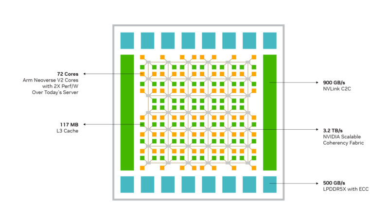
For all of the success of Grace in terms of units shipped and general goodwill for NVIDIA, the chip has one competitive pitfall for the company: the underlying CPU cores are not an NVIDIA design. For their first data center chip design, NVIDIA played things relatively conservatively a licensed an off-the-shelf core design from Arm, tapping the company’s Neoverse V2 core to be the centerpiece of their taskmaster chip. In the intervening years, Grace has become one of the most important Neoverse V2-based chips on the market. But it is not the only Neoverse V2 chip; it is not a technology that NVIDIA can exclusively provide.
For this and several other reasons, NVIDIA has gone back to the drawing board for Vera. Rather than using a licensed CPU design for their second data center chip, NVIDIA has designed their own Arm v9.2-A CPU core from scratch: Olympus. This marks the first time that NVIDIA has designed their own CPU core since the last of the Denver cores was released almost a decade ago.
Compared to using an off-the-shelf design, going with a custom CPU core design is a more aggressive route that comes with additional risk (they are building and validating an entire CPU core, after all). But the potential payoff for NVIDIA is significant on both the technological front and the financial front.
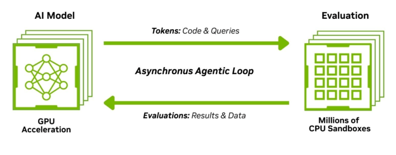
In terms of technology, NVIDIA has been able to build a chip that is better tuned to their specific needs – which in this day and age is all about AI. As NVIDIA tells it, a big part of the impetus behind Vera’s design is that NVIDIA wanted a faster CPU for quickly handling reinforcement learning tasks as well as all of the conventional compute workloads spawned by agentic AIs.
Meanwhile on the financial front, the total costs of licensing just the Arm architecture are cheaper than licensing one of Arm’s premade CPU core designs. Royalties in particular are a huge factor here, as custom chip designers like Apple, Qualcomm, and now NVIDIA pay much less than they would using Arm’s designs. And, of course, because the Olympus core is a custom design, NVIDIA’s hardware is that much more differentiated from the competition – which in turn gives NVIDIA a market opportunity to sell this hardware to other customers if the performance is good enough.
A Look at Vera: NVIDIA CPUs Embrace the Chiplet Era
While NVIDIA first outlined Vera back at CES 2026 alongside the rest of the Vera Rubin platform, the CPU is getting a seconding coming out party at GTC 2026, where NVIDIA is formally launching the CPU. Alongside this, NVIDIA has been disclosing some additional architectural details about the chip for the first time.
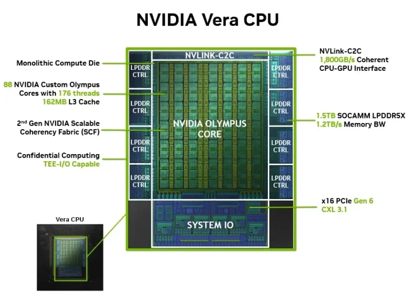
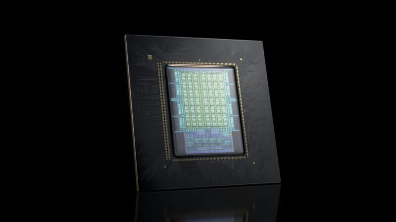
For a start, Vera is a chiplet-based CPU design. Specifically, Vera is comprised of a single CPU compute chiplet that is further surrounded by multiple chiplets for I/O and memory.
While the total chiplet count is unconfirmed by NVIDIA, by our count we are looking at a compute chiplet (with NVLink C2C functionality), four memory chiplets, a pair of spacers, and then a single I/O chiplet providing PCIe and other connectivity.
Comparing and contrasting this to other data center CPU designs – most notably from AMD and Intel – NVIDIA’s design is similarly disaggregated in function. But critically, it does not involve splitting up the compute core/CPU blocks in any way. Whereas an AMD EPYC design will have upwards of 16 CPU chiplets and then a central I/O die, or an Intel Xeon design will pair multiple I/O tiles with up to 3 compute tiles, NVIDIA keeps the entire compute core – all 88 CPU cores – as one chiplet.
In fact, this is something that NVIDIA is promoting as a feature benefit for Vera. Because of its singular compute chiplet, NVIDIA has not needed to employ NUMA domains or other partitioning with the chip. All of the CPU cores have fast and ready access to each other, as well as other resources such as the memory controllers. The end result is that Vera is closer to functioning as one large CPU, for all the benefits and drawbacks that entails.
Still, compared to Grace before it, this is NVIDIA’s first disaggregated CPU design. Moving the memory controllers and I/O to separate chiplets is relatively simple in comparison, but it goes to show how popular and common this technique has become. There are few (if any) good reasons these days to have I/O and memory controllers eating up expensive leading-edge silicon when something older (and cheaper) will do.
| Feature | Grace | Vera |
| CPU Architecture | Arm Neoverse V2 | NVIDIA Olympus |
| Cores | 72 | 88 |
| Threads | 72 | 176 (Spatial Multithreading) |
| L2 Cache per core | 1MB | 2MB |
| Unified L3 Cache | 114MB | 162MB |
| Memory bandwidth (BW) | Up to 512GB/s | Up to 1.2TB/s |
| Memory capacity | Up to 480GB LPDDR5X | Up to 1.5TB LPDDR5X |
| SIMD | 4x 128b SVE2 | 6x 128b SVE2 FP8 |
| NVLINK-C2C | 900GB/s | 1.8TB/s |
| PCIe/CXL | Gen5 | Gen6/CXL 3.1 |
Its single NUMA domain aside, the other notable memory-related aspect of Vera is just how much memory bandwidth it has access to: 1.2TB/second for the entire chip. With a 1024-bit LPDDR5X memory interface enabled by the use of 8 SOCAMMs, Vera has access to far more memory bandwidth than contemporary CPUs from Intel or AMD. On a per-core basis this works out to almost 14GB/second of memory bandwidth, which is a generation ahead of contemporary Intel and AMD designs. And for NVIDIA, this is a critical aspect to keeping those high-performance Olympus CPU cores fed.
The Olympus CPU Core
The star of the show that is Vera, NVIDIA’s Olympus CPU cores are designed to be performance monsters. With NVIDIA offloading as much parallel, latency-insensitive work to their GPUs as they realistically can, the company needs a high-performance CPU to handle all of those serial, latency-sensitive tasks that their GPUs cannot. This is the same general role that Grace has filled for the last few years, but with two generations of GPU upgrades since Grace came around – Blackwell and now Rubin – NVIDIA’s CPU performance needs are increasing as well.
Consequently, Olympus has been designed to be a very high IPC architecture. NVIDIA is targeting 1.5x the IPC of Grace, which compared to other chip architectures is a major IPC jump in a single generation – albeit tempered by the fact that it is been nearly 4 years since Grace was released. To get there, NVIDIA is building a very wide front-end, which the company is now confirming has a 10-wide instruction decoder, which can allow Olympus to decode and generate a relatively high number of operations if the decoder can be filled. Compared to existing architectures this is wider than both Zen 5 (8-wide) and Granite Rapids/Redwood Cove (6-wide), and is similarly wider than the 6-wide instruction decoder of Neoverse V2.
Olympus’s hefty frontend also contains dual branch predictors, allowing the CPU core to spit out two branch predictions per cycle. Which, in turn, are generated by what NVIDIA is calling their neural branch predictor.
Unfortunately, NVIDIA has been far less forthcoming on the backend resources available in Olympus. But according to the company’s CPU core software optimization guide, there looks to be at least 14 pipelines for handling integer and floating point/SIMD operations – and other pipelines still for load/stores and such. All of which indicates that NVIDIA has paired Olympus’s sizable frontend with a similarly enormous backend.
Which in turn is why, as we learn more about Olympus’s architecture, that NVIDIA’s implementation of simultaneous multithreading on Olympus does not just schedule multiple threads on a single CPU core. Rather, it fully partitions the CPU core. Dubbed spatial multithreading, NVIDIA foregoes the timesharing nature of traditional SMT in favor of giving each thread a fixed and reduced set of resources. The resulting trade-off for system operators, then, is whether to allow more threads at reduced throughput (but perhaps better overall utilization of the hardware) or fewer threads moving through the Olympus cores as fast as the hardware can take it.


This is to Patrick: Can you please ask your new writers, as good as they are, to properly review and spell check. Here’s one example I picked up: NVIDA
This site has a reputation for excellent reviews and well written articles, many others and I would like to see it kept that way.
I forgot to add, the positive not to this, is that they’re hand writing their articles :-)
@Mick
Thank you for the feedback. That one is my bad.
These do get spell and grammar checked (and I am probably harder about that than anyone else here at STH). However MS Word does not check words that are written entirely in capital letters, as those are normally acronyms that wouldn’t be in a dictionary. Which means it didn’t flag that misspelling of NVIDIA. Normally, if I screw up NV’s name it’s as “NVIIDA”, so I didn’t catch that more novel misspelling.
Best Vera write-up I’ve seen so far. And good to see Travis Downs writing again on that RedPanda blog….but…that blog is not ideal. In particular, the lack of any specs on the parts tested. You know how wide the performance delta on Epyc and Xeon within the same generation are based on what sku was used (even if testing on the same number of cores). Yet, nothing was included on overall core count, TDP, etc. So is hard to draw any conclusions just yet. Even basic things like was this with or without Nvidia’s “SMT”.
@Mick The irony is that you have a spelling mistake in your second post…
“the positive not to this”, do you mean the positive note or the positive nod?
@Blue4130
Yeh I saw that right after I posted it, real foot in mouth moment.
It was indeed mean’t to be “…the positive note to this….”
In a world of AI Slop, this site is one of the last bastions. Half the time I google for a review of a product, I’ll click on a given link and what I’ll find is an AI generated review with no actual views, opinions or anything.
>In a world of AI Slop
@Mike, I hope you do realise Ryan Smith was the Chief Editor at Anandtech for 10+ years before it was shut down.
The spatial multithreading reminds me of AMD’s Bulldozer . The front end here is huge as compared to Bulldozer so the backend should not be starved. but the performance gap between a single beefy core and split core is big enough to confuse most schedulers.
The latest linux patch from Nvidia suggest that they are seeing issues similar to bulldozer.