
Samsung took the stage at Hot Chips 2026 to present LPDDR5X-PIM, a processing-in-memory memory solution built on LPDDR5X DRAM for AI inference. This is one that several folks outside the theatre were hotly anticipating today.
We are covering this talk live, so please excuse any typos.
Samsung LPDDR5X-PIM at Hot Chips 2026
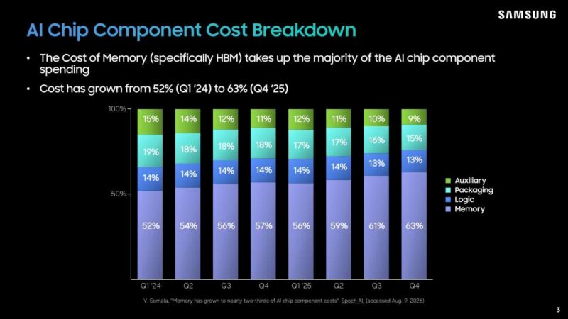
Samsung opens with a market-context figure that frames its pitch around memory cost as a percentage of AI packages. HBM now claims the majority of AI chip component spending, and that share grew from 52 percent in Q1 2024 to 63 percent by Q4 2025. It is likely higher now.
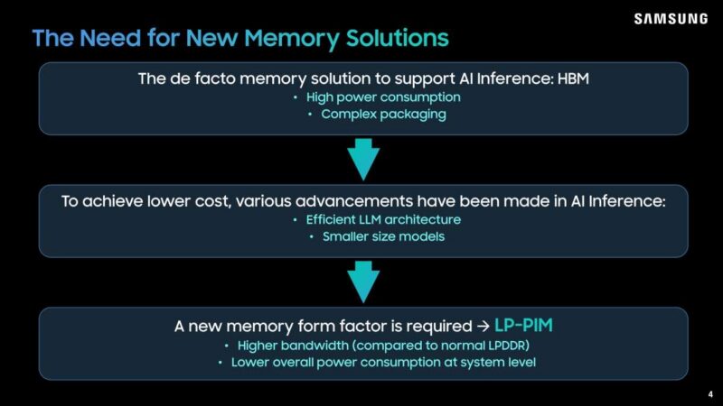
HBM delivers the bandwidth AI inference needs, but with high power consumption and complex packaging. Samsung argues the route to lower cost runs through a new memory form factor the LP-PIM.
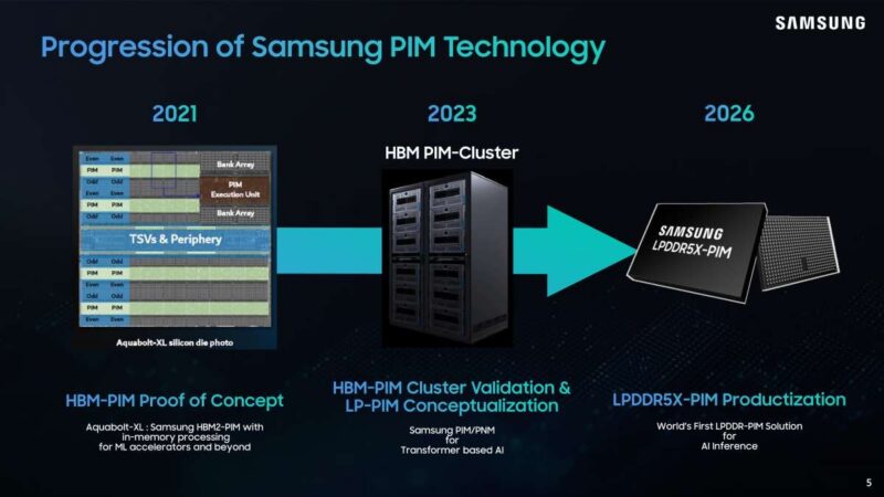
Here Samsung traces its PIM timeline, from the Aquabolt-XL HBM2-PIM proof of concept in 2021 through LPDDR5X-PIM productization in 2026 as the world’s first LPDDR-based PIM solution. You can read our pieces on Samsung HBM2-PIM and Aquabolt-XL at Hot Chips 33 and Samsung Processing in Memory Technology at Hot Chips 2023.
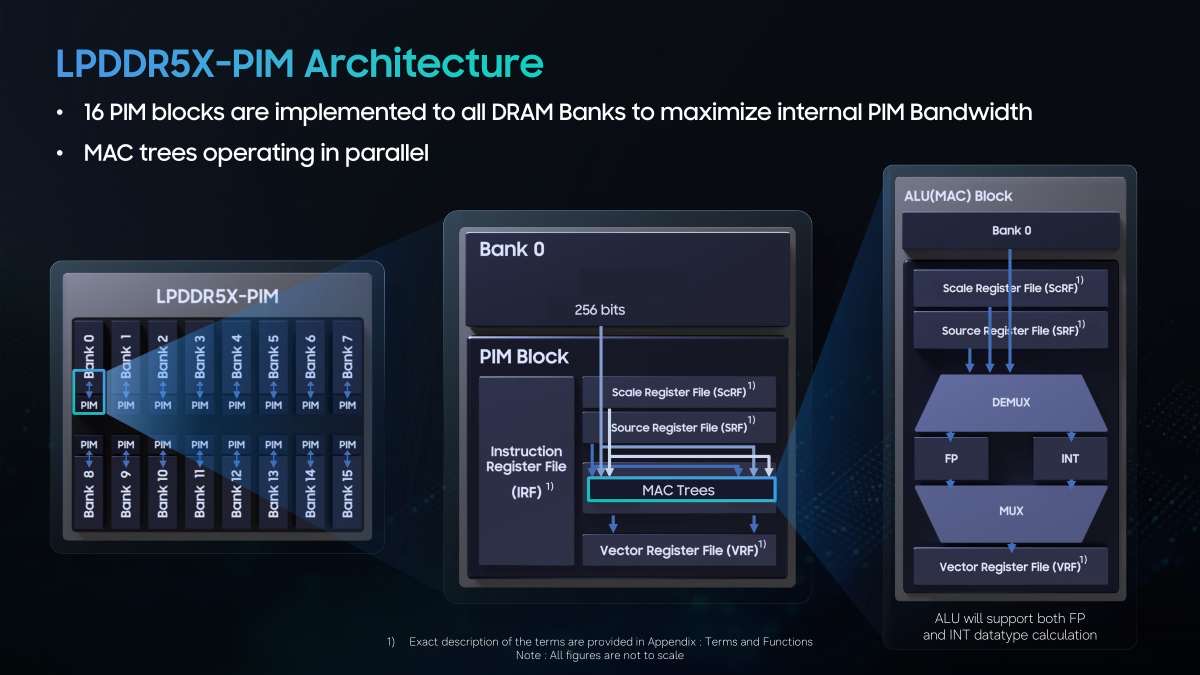
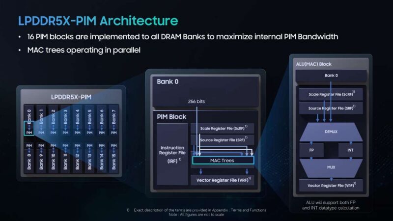
Now to the LPDDR5X-PIM architecture itself. Sixteen PIM blocks sit in the DRAM banks, with MAC trees running in parallel and an ALU that handles both FP and INT data-type calculations.
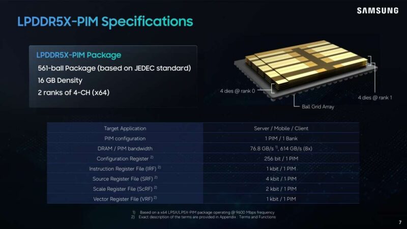
This specification figure shows a JEDEC-standard 561-ball package with 16 GB across four dies per rank, targeting server, mobile, and client. PIM bandwidth reaches 614 GB/s at the x64 9600 Mbps operating point, eight times the 76.8 GB/s available on the conventional DRAM side.
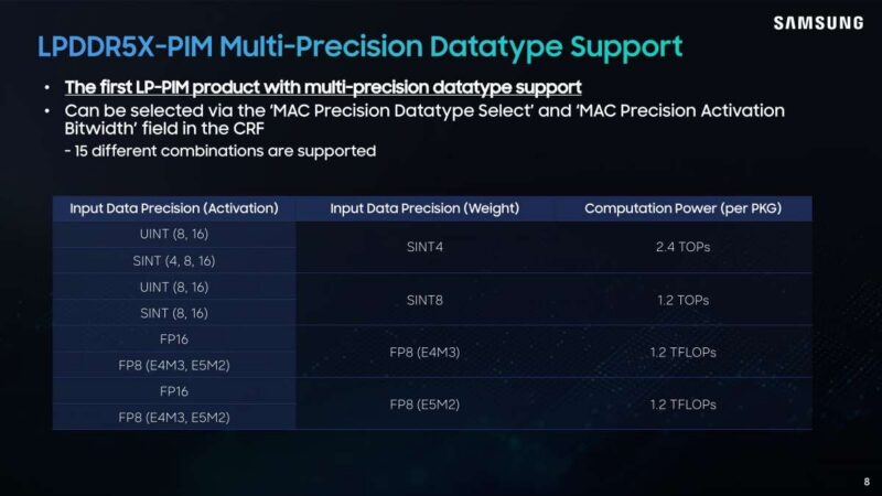
LPDDR5X-PIM is the first LP-PIM product with multi-precision data type support. Fifteen combinations are selectable through the MAC precision fields in the configuration register. Activations can pair with SINT4 weights for 2.4 TOPS, or fall back to roughly 1.2 TFLOPs per package in FP8.
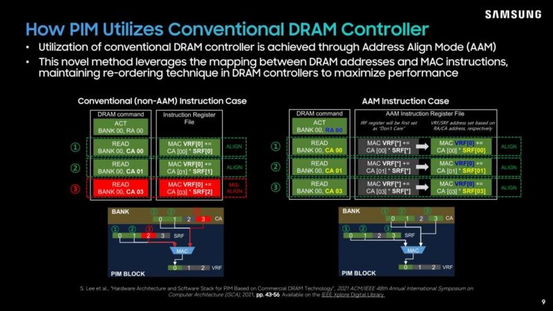
Drop-in compatibility rests on Address Align Mode. This mapping between DRAM addresses and MAC instructions lets LPDDR5X-PIM work with a conventional DRAM controller rather than requiring a new one.
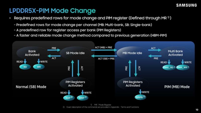
Mode change shuttles the part between single-bank and multi-bank PIM operation. Predefined rows and PIM registers handle the switch, and Samsung says this method is faster and more reliable than the HBM-PIM approach of prior generations.
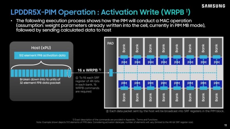
Activation write begins the MAC flow. Sixteen WRPB commands fill the source register files across the banks with FP8 activation data broadcast from the host.
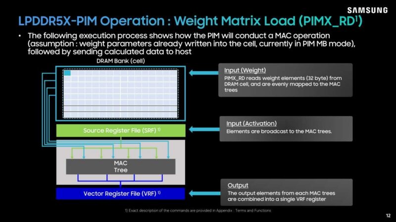
Next, the weight matrix loads. PIMX_RD reads 32-byte weight elements from the DRAM cell, maps them across the MAC trees, and combines the outputs into a single vector register file.
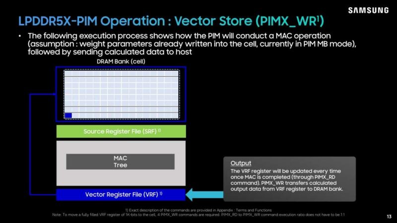
Partial sums are written to the vector register file as each MAC completes. PIMX_WR then moves that data back to the DRAM bank, and the read-to-write ratio is free to vary rather than being locked at 1:1.
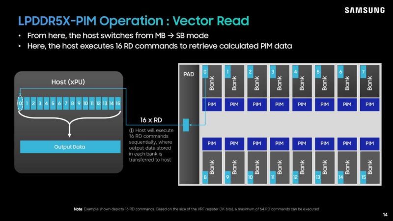
To pull results back, the host switches to single-bank mode and issues sequential RD commands. A maximum of 64 such reads serves the 1-kbit vector register file.
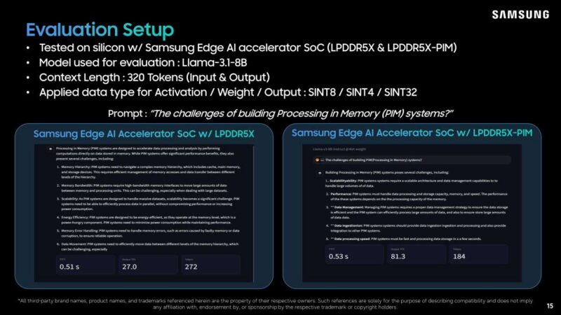
Samsung validated the design on silicon. This evaluation used its edge AI accelerator SoC with both LPDDR5X and LPDDR5X-PIM, running Llama-3.1-8B with a 320-token context, SINT8 activations, SINT4 weights, and SINT32 output.
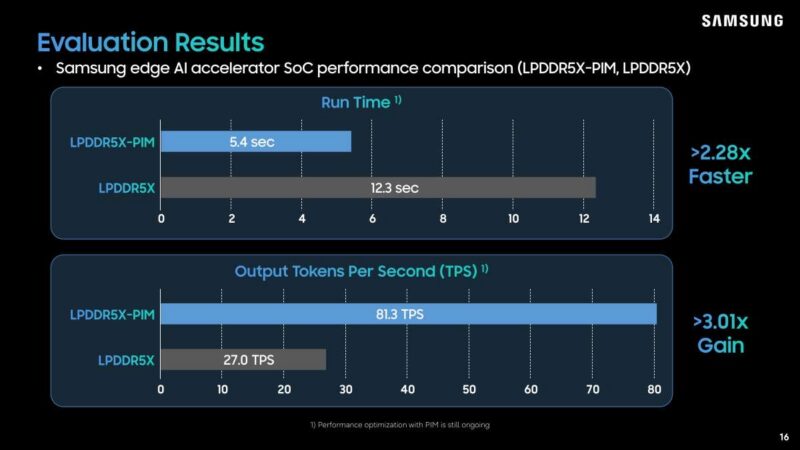
This LPDDR5X-PIM build finished the run in 5.4 seconds against 12.3 seconds on conventional LPDDR5X, a 2.28x gain, and output climbed to 81.3 tokens per second from 27.0, a 3.01x gain. That is a big part of the value proposition.
Samsung made clear that software is part of the package. A simulator and datasheet are available on request, and the SDK bundles reference tooling, while LPDDR6-PIM moves toward a finalized JEDEC LP6-PIM specification.
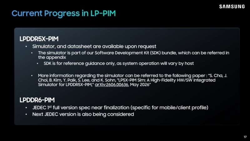
The JEDEC step seems like a big step on the way from a research project to a shipping product.
Final Words
Samsung is positioning LPDDR5X-PIM as a lower-cost, lower-power alternative to HBM for AI inference, and the measured gains on its edge AI accelerator make that pitch concrete. This one feels like one where a large customer is going to have to come in and say this is needed, implement it, and then it will get widely adopted. Perhaps the challenge is that if you give a memory vendor not just control over the memory but also the compute side, they have more leverage with their customers. You need standardization at least so a vendor can second source.
We have a full recap on the Substack, including where all of these pieces ranked in terms of popularity: