There is a new 3D NAND vendor on the block. Yangtze Memory Technology Company or YMTC is launching 3D NAND technology it calls Xtacking. Traditionally the NAND market has been dominated by companies like Samsung, Micron, Toshiba, and others. As part of the Made in China 2025 program, YMTC is using a state-backed production facility to produce NAND. The goal makes sense, China sees that the major semiconductor companies are outside of its borders and wants to invest in its industry.
About YMTC Xtacking
Here is the background on YMTC Xtacking from the company’s site:
Xtacking enables DRAM-like high I/O speed
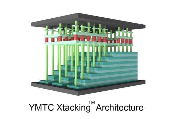
With Xtacking, the periphery circuits which handle data I/O as well as memory cell operations are processed on a separate wafer using the logic technology node that enables the desired I/O speed and functions. Once the processing of the array wafer is completed, the two wafers are connected electrically through millions of metal VIAs (Vertical Interconnect Accesses) that are formed simultaneously across the whole wafer in one process step, using the innovative Xtacking technology, with limited increase in total cost.
Xtacking enables higher array efficiency
In the conventional 3D NAND architecture, the periphery circuits take up ~20-30% of the die area, lowering NAND bit density. As 3D NAND technology continues to progress to 128 layers and above, the periphery circuits will likely take up more than 50% of the total die area. With Xtacking, the periphery circuits are now above the array chip, enabling much higher NAND bit density than conventional 3D NAND.
Xtacking: Modular approach to accelerate process development and shorten manufacturing cycle time
Xtacking technology utilizes fully independent processing of the array and periphery, which offers a modularized, parallel approach to product development and manufacturing, reducing product development time by at least three months and shortening manufacturing cycle time by 20%, significantly accelerating 3D NAND time-to-market. This modular approach also opens possibilities for customized NAND flash solutions by the incorporation of innovative functionalities in the periphery.
The New York Times noted that parts of YMTC NAND look extremely similar to Samsung NAND in their piece Inside a Heist of American Chip Designs, as China Bids for Tech Power.


It’s easy to have a press release – not so much to actually ship a product. Get back to me when any of these claims are proven.
I had about the same thoughts when they took over Volvo, now it is the 4th premium brand next to Mercedes, BMW and Audi and they grow faster than the other two brands. Don’t underestimate the Chinees. Same story with HPC, they can do it themselves these days.