
Microsoft presented its new infrastructure developments at OCP Summit 2018. Last year, the buzz was around Project Olympus which was successful and deployed in Azure. This year, Microsoft’s contributions are focused on security and storage. We wanted to highlight Microsoft Project Denali for flash storage which may have major repercussions in the storage industry.
Microsoft Project Denali Background
Starting out the background information, Microsoft threw out some numbers. 30% of global flash output consumed by enterprise and cloud. Of that 30%, half is consumed by big cloud companies or roughly 15% of global output. Of that amount, Microsoft consumes “multi-exabytes” of flash storage each year. The message behind this is that Microsoft and other hyper-scalers are huge consumers of NAND flash and that it is a technology that makes up a large portion of the Azure infrastructure.
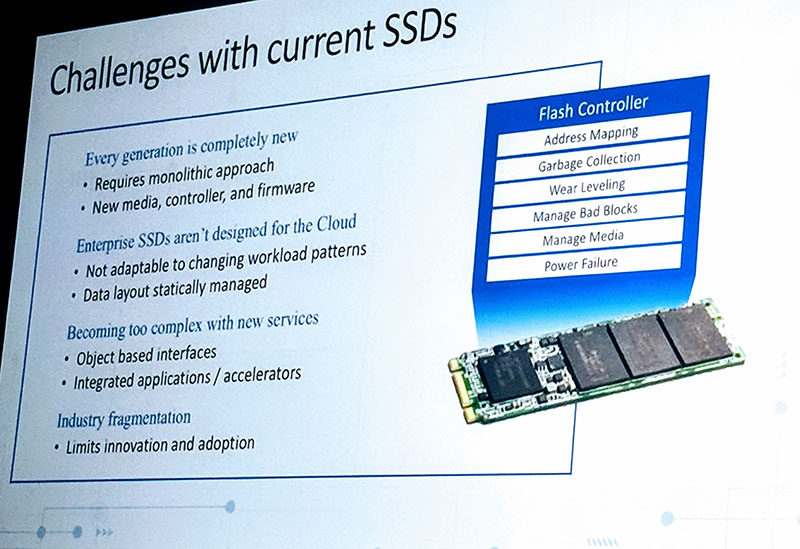
Since it is a large part of the Azure infrastructure, Microsoft sees challenges with the current generations of SSDs. Most of these challenges boil down to the fact that SSDs are designed as a tight product between the NAND, controller, and firmware rather than being seen as raw storage to a larger software-defined paradigm.
Microsoft acknowledged that every SSD supplier is driving innovation, but not necessarily in the same way. Project Denali is designed for cloud-first storage. Microsoft wants to be able to take advantage of new NAND and storage class memory as it becomes available. As such, it needs to disaggregate the current storage model and use software-defined data placement that works in tight coordination with the SSD.
Project Denali has focused on four main goals:
- Flexible architecture for innovation agility: Workload-specific optimizations, FTL managed as cloud services component
- Rapid enablement of new NAND generations: NAND follows Moore’s Law; SSDs: hours to precondition, hundreds of workloads
- Support a broad set of applications on massively shared devices: Azure (>600 services), Bing, Exchange, O365, others; up to hundreds of users per drive
- Scale requires multi-vendor support & supply chain diversity: Azure operates in 38 regions globally, more than any other cloud provider
(Source: Microsoft Azure)
Microsoft Project Denali Disaggregates Flash Model
Microsoft Project Denali is designed for the disaggregation of flash storage. Instead of all of the address mapping, garbage collection, and wear leveling happening on the SSD itself, Microsoft thinks that its Azure cloud workloads would be better serviced by managing the data placement at a higher level.
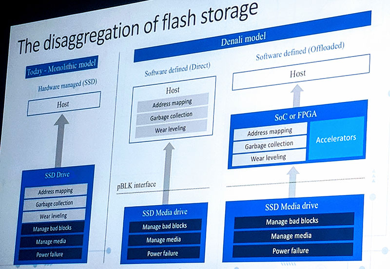
In this new paradigm, SSDs would still be responsible for the raw media layer, taking care of ECC and bad blocks. The new job of SSDs will simply be to present “perfect NAND” to the software layers above. Perfect NAND can be simplified is an array of NAND at a certain latency.
Microsoft thinks software can define address mapping, garbage collection, wear leveling. This is because it believes the application knows the workload pattern the best and can decide how to lay out the data on the device. Making applications or higher-level software aware means that software can be used to lower write amplification, lower costs, and better performance by exposing parallelism. Using this model, SoCs or FPGAs can be used to accelerate the storage tasks across broader arrays of NAND.
To the SSD vendors, this should sound terrifying. Many of the functions that these vendors use to differentiate essentially move up the software stack. If an SSD or NAND provider needs to only ensure that it is presenting NAND that is functional and will retain data, then it lowers the intelligence and value SSD vendors can deliver. Microsoft knows this and if you were looking to push cost out of a large deployment, this is one way you can do it.
Project Denali Prototypes to m.2 Deployment
This is a project that has been ongoing for years. Microsoft, Dell, Micron, Samsung, Seagate and others all have investments in a company, CNEX Labs that has been the primary developer of the new storage class. Over the years, it has provided a few different prototypes of what these devices can look like.
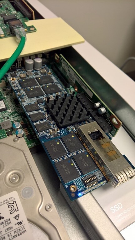
On stage at OCP Summit 2018, we got our first glimpse of the first m.2 drive in the hand of CNEX Labs co-founder Alan Armstrong.
Those in attendance were told that this new m.2 form factor will be deployed in data centers this year. As you can see, the form factor has been miniaturized and better productized. Also, with deployment only months in the future, Project Denali is moving from the theoretical prototype space to something in use by potentially millions of customers in the next few quarters.
Other Perspectives on Project Denali
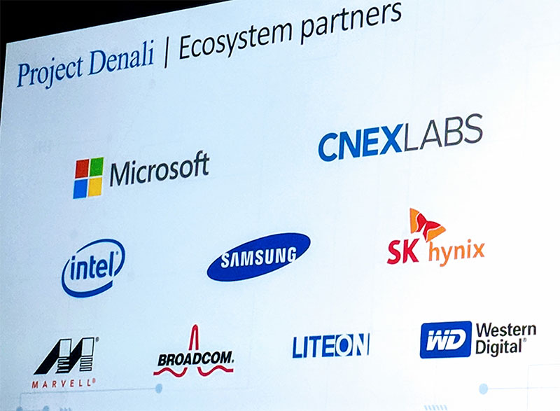
There are many implications of this technology, especially in the ecosystem. On stage, the companies were able to list a number of prominent partners for the project.
At the show, we asked several of the vendors what they thought of this. There was some concern over how much IP the NAND makers would have to share to make this work. Likewise, Microsoft is such a large flash buyer that this was seen as something that may end up being fact on that account.
While editing this article, we were able to speak to Robert Hormuth, CTO, VP/Fellow, Server & Infrastructure Systems at Dell EMC. His 30-second take is that this is certainly an interesting technology, but it is not quite ready for enterprise customers in its current form. He also said that Dell EMC is keeping an eye on the technology as it matures and will continue to evaluate it going forward.
We asked other hyper-scalers who were at the conference and they said they are interested to see what else comes from the project.
Final Words
We do not see this as taking over the consumer market or the lower-end enterprise market anytime soon. If you are dealing with a small number of devices and fewer users/ applications, the current model is both well understood and works well. Instead, we see this as a cost and performance push by the hyper-scale players as it leads to the commoditization of hardware. At the same time, for a large hyper-scaler like Microsoft that has CPU and FPGA fabrics widely deployed, Project Denali makes sense as a next-step solution for lowering costs and extracting value from a massive scale.


Smells an awful lot like what Pure Storage has been doing for years: move the brains of a bunch of SSD’s to controller-heads, instead of having a brain in each individual device. Just on a much larger scale.
I knew this is coming sooner or later once Intel has release CPU + FPGA.
Next step put FPGA next to nand to reduce IO.
@Steve–But even Pure keeps it in hardware, right? They’re move it from the SSD to the controller, where the controller firmware handles the wear-leveling, etc. Looks like Denali wants to make all of the hardware dumb, and let the OS manage the NAND.
@ Rob. Pure too uses the raw power of modern server-grade CPU’s. I cannot think of anyone using ASIC’s anymore. Even big guns like the mighty EMC VMAX are based on Xeon’s.
The linux kernel also has support for this type of memory, I believe it’s called LightNVMe or Open Channel SSD. I don’t think the term “commoditization” and “hyperscaler” mesh very well, in fact we’re seeing that a lot more Hardware options are made available to these companies first or even only.
What Nils said. Open Channel SSD’s are nothing new. The research and support for it has been going on for decades in the Linux world. It resulted for instance in the LightNVMe standard, an addendum to NVMe standard. The normal form factor for these devices is U.2, that is a 2.5″ SATA/SAS form factor that runs PCIe on the connector. Alibaba is so big, that they manufacture these devices themselves for their own cloud as can be read here: https://www.alibabacloud.com/blog/alibaba-deploys-alibaba-open-channel-ssd-for-next-generation-data-centers_593802
The real reason that SSD’s are super intelligent is primarily to be software compatible with disks. Just like SATA controllers emulate IDE controllers, and IDE controllers (actually the disks, as IDE itself is almost just a parallel port) emulate the WD1003 mfm harddisk controller, just to make it easy on the software.
Or imagine the 64 bit cpu’s booting in x86 16 bit real mode… Oh wait, that actually really happens: “As of 2018, current x86 CPUs (including x86-64 CPUs) are able to boot real mode operating systems and can run software written for almost any previous x86 chip without emulation or virtualization.” (real mode article on wikipedia).
So hardware innovation? Not so much, and mostly due to lagging software. Yeah, you know specifically what software we talk about.
Comments are closed.