
As part of every major processor launch, we like to have our architecture overview piece. With the introduction of the Intel Xeon D-2100 series, Intel brings a flavor of its Skylake generation cores together with enhanced platform-level enhancements to bring a major new solution to market. Intended for edge deployments, this is a newer, more expandable and more powerful solution than the Xeon D-1500 series. In this article, we are going to cover the architecture and platform of the new Skylake-D generation Xeon D family.
Intel Xeon D-2100 Microarchitecture Refresher
One of the biggest reasons for the existence of the Xeon D product line is to serve as an instruction set compatible edge computing platform. As such, Intel needed to release an updated part that matches much of the functionality of the Intel Xeon Scalable family codenamed Skylake-SP. You can read more about the microarchitecture in-depth, but we wanted to highlight a few key points.
First, the new chips have switched to the newer mesh interconnect. This makes perfect sense as the L2/ L3 caches and home controllers have been aligned to the Skylake-SP generation with the 1MB / 1.375MB split between L2 and L3 caches.
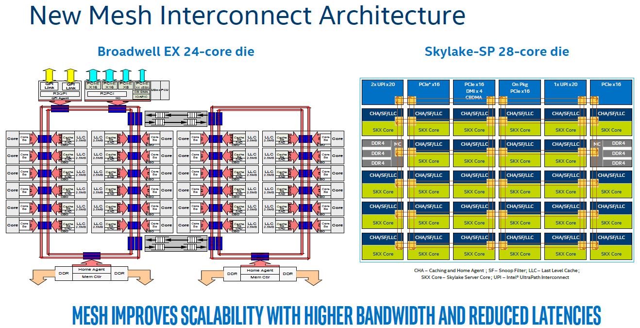
The cores themselves will be similar to the Skylake-SP cores and have features such as updated Turbo boost which can handle per-core boosting and faster transitions between states than previous generations.
The actual instruction set has been updated to align with the Skylake-SP generation as well. This is important for customers who want their applications to run identically on the edge as they do in the primary data centers.
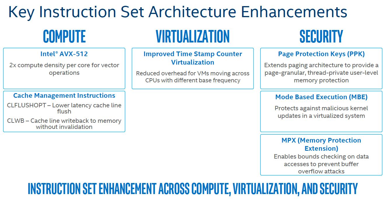
A key point here is that the new Xeon D-2100 series only has the single port FMA solution similar to the Intel Xeon Bronze, Xeon Silver, and Xeon Gold 5100 series. What that means is that while the new edge SoCs can execute the AVX-512 code, they do not have the same compute capacity as the higher end Xeon Scalable parts.
Intel Xeon D-2100 Series Architecture and Platform
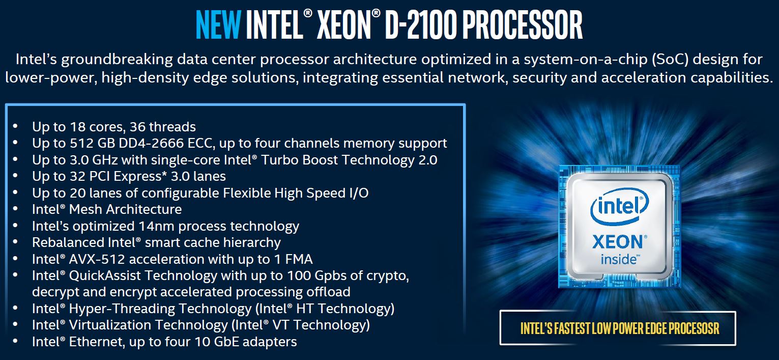
In terms of raw features, we have the standard Skylake-SP cores but there is much more to the platform. Here is Intel’s platform-level overview:
We wanted to highlight a few bits. First, there are now four memory channels instead of two on the Xeon D-1500. The memory capacity has jumped from 128GB maximum on the Xeon D-1500 series to 512GB now using 8x 64GB LRDIMMs. What is interesting is that a number of vendors are claiming 128GB DIMM support which would imply 1TB memory support. That would conflict with the lower 768GB memory cap of mainstream Xeon Scalable.
In terms of networking, all but the top end 18 core SKU have 4x 10GbE Ethernet. The MAC for this networking comes from the Intel X722 family of controllers which means that there is excellent OS support for this as it aligns with the Xeon Scalable PCH SKUs. Also aligning with the latest PCH generation is the ability to have QuickAssist Technology enabled SKUs. There are 100Gbps, 40Gbps and 20Gbps QAT options with the Xeon D-2100 series QAT SKUs.
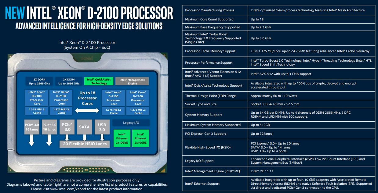
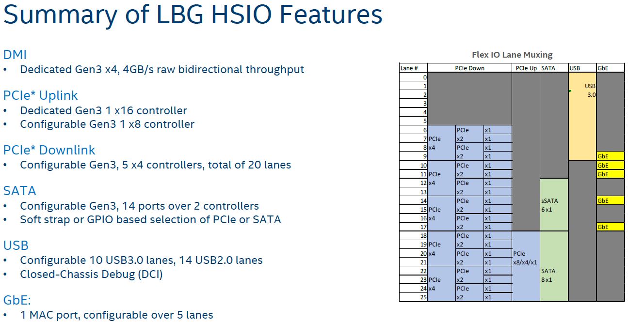
In terms of the platform I/O, there is a major generational difference again matching the Lewisburg PCH. With this generation, there is a greater focus on PCIe connectivity. There are two PCIe 3.0 x16 hubs available for 32x PCIe 3.0 lanes total. Beyond this, there are 20 HSIO lanes that can be used for additional PCIe (20), SATA III (14) or USB 3.0 (4). This is similar to the Intel Atom C3000 series SoCs as well.
Origins Lewisburg?
We are not yet sure how the Xeon D-2100 is put together. If one looks at the Lewisburg PCH family, one will notice a striking similarity between the platform features of Xeon D-2100 and the Lewisburg PCH family.
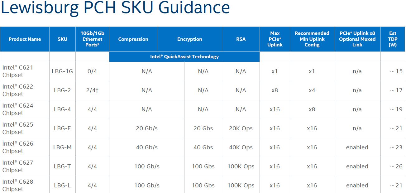
The 4x 10GbE, optional Quick Assist and the ability to provide downstream I/O are present with Lewisburg. Likewise, the 20x downstream PCIe 3.0 lanes, or up to 14 SATA III lanes match the Xeon D-2100 specs.
For those deploying the Intel Xeon D-2100 this is great news as it minimizes the number of drivers which is a net positive no matter if the PCH functionality is integrated on silicon or simply that there is a Lewisburg PCH on the same package.
A lot of technology geeks are going to question whether this is indeed a true SoC or a package made up of a Xeon Scalable die plus a Lewisburg PCH. While from a cost standpoint there are implications, what matters to embedded customers is that the packaging is smaller without the LGA3647 socket plus a seperate PCH.
Final Words
There are a few architectural themes that are important to remember. Compared to previous generations and the Intel Atom C3000 series, there is a greater emphasis on matching the Xeon Scalable instruction set and expanding I/O and memory. To handle all of these enhancements, TDPs are up significantly with a range of 60-110W. If you compare this to Xeon D-1500 series which could get into 25W SKUs and where the primary compute SKUs topped out at 65W, it is clear that Xeon D’s title as the low power performance option is diminished.
At the same time, if you were looking to build more robust edge compute, network, and storage infrastructure, the new Intel Xeon D-2100 series is going to be a major upgrade if you need a smaller form factor. If you can tolerate a larger form factor, even more consolidation can occur by stepping up the full-scale Xeon Scalable line.
If you want to read more about the new product family, check out our Intel Xeon D-2100 launch coverage central.


Rather disappointed about the networking options. I would have liked at least 40GbE, leaving the PCIe lanes for NVMe.
Does Intel Xeon D-2100 need the OS relocation?
Correction: Does Intel Xeon D-2100 need the OS kernel relocation?
Are OS patches, if needed, ready for it?
Given that it’s Skylake it is still vulnerable to Meltdown as well as Spectre.
Comments are closed.