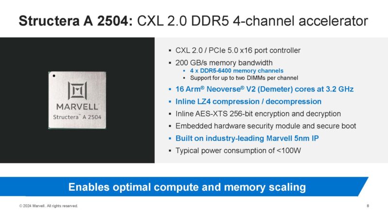
Marvell Structera A 16-core Arm and DDR5 Chip
Let us get a bit more exciting and take the Structera X 2504 up a notch by adding sixteen Arm Neoverse V2 cores. These are high-performance Arm cores like you would see in a NVIDIA Grace CPU, but just on a CXL accelerator. That is what makes the Marvell Structera A a different animal.
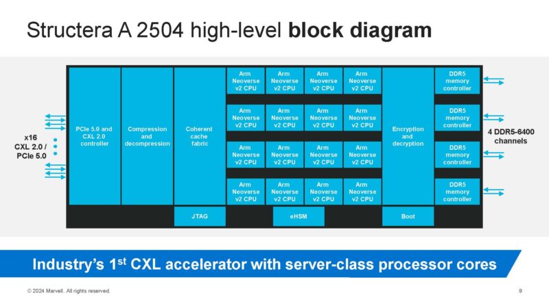
Taking a look at the block diagram, this is just like the X 2504, but the A 2504 has the Arm Neoverse V2 cores in the mdidle.
If you are wondering how this works in practice, think of it like there is a lightweight Linux distribution running onboard this as an endpoint. That makes this like a mini-server in another server that is designed to run at the speed of memory. Fast Arm cores where the goal is to do compute on the attached memory.
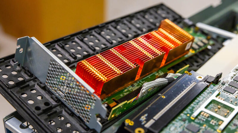
The cards we saw these on in the lab had DDR5 packages on both sides of the cards that were in low profile x16 form factors.
If you need a mental model of how this works, think about it like a DPU, but instead of processing networking flows, it is designed to work on its local memory. That means one can scale both memory and compute in a server at the same time. Of course, the fun part of going to Marvell is that we got to see a live demo.
The CXL Can Be Fast Demo
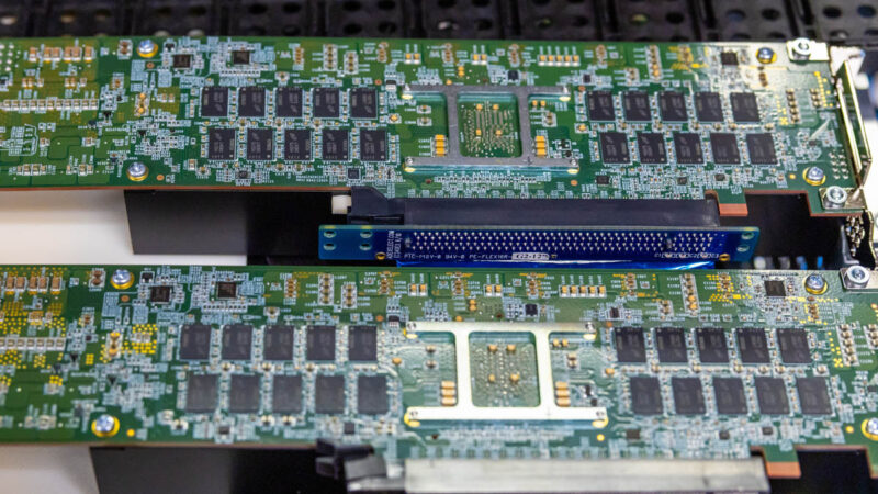
Folks know that at STH I prefer to show the behind the scenes instead of perfectly curated images. Take Exhibit A in that journey: the CXL Demo Rig. THis is one of the systems with Structera A 2504 cards with a Supermicro Intel Xeon Server, an Antec power supply, a few fans, and lab-appropriate wiring.

The other demo rig looked quite a bit better.
In the video we showed the demo, but we showed the Structera X acting as storage for KV cache when the GPU would have otherwise run out of memory. This was effectively telling a Llama 3 model to read books, then ask questions about the books.
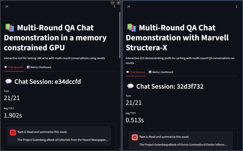
The model was still running on the GPU, but just being able to have the KV cache stored in memory changed the time to first token. The runs varied a bit, but when you do many runs the TTFT saved us about 30 seconds total. Of course, this really just saying having more memory is good even if the latency is a bit higher.
Still, I wanted to know how the Structera A worked. Here is a fun one. You can see the left system where a search is running 48 Intel Xeon cores and the local memory attached to the Xeon socket.
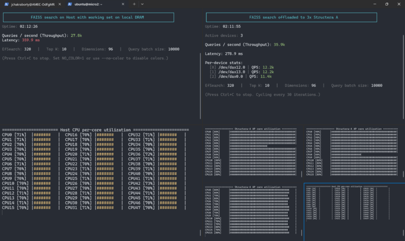
On the right hand side, we are logged into the three Structera A cards that are running near 100% utilization and then the Xeon cores are not loaded at all (in the bottom right corner.) The idea with this demo is that we have 48 Arm Neoverse V2 cores across the three cards. With the Xeon cores free, the system can do more by scaling memory with the added compute.
These were demos that were really focused on showing off how the modules can be used for performance benefits, but there are a number of use cases where having more memory, or more memory and compute in a system can add more performance.
Final Words
This was a neat look behind-the-scenes at a technology that is being used at hyper-scalers. From an industry perspective, this idea was one that started at one hyper-scaler but almost all are now using, especially since they see the benefits from recycling their DDR4.

The Marvell Structera is currently focused on those hyper-scale projects which makes sense. Recycling DDR4 or adding DDR5 is easier when there are a limited number of host systems, module types and so forth. Just getting all of the firmware to work is one of the reasons we do not see commercially available CXL expansion devices. Structera A also requires managing the Linux distribution on the cards, sending commands to the Arm cores, and so forth. Still, this is super-cool technology that is being deployed at hyper-scalers and that we do not get to see often. Hopefully the STH community likes seeing these behind-the-scenes lab visits.


Without third-party testing of latency, bandwidth and latency while being bandwidth bottlenecked it’s difficult to know whether this is useful or not.
I’m curious how the additional uncertainty introduced by memory compression is handled. A lot of real world data is amenable to lossless compression; but not all to the same degree and some not at all.
Is the compression visible to the OS and its memory allocation mechanism; with that responsible for deciding how much compression to expect and how to respond if that expectation proves optimistic and there isn’t as much physical RAM as required? Is it invisible to the OS and the CXL device presents itself as larger than the physical RAM with a margin of safety chosen to make hitting enough incompressible data to run out unlikely?
After reading this article, I instantly became bloated with an unbearable amount of gas buildup leading to an unequivocal paradox of methane emissions. This has lead to fecal aerosol toxicity levels of astronomical proportions in my proximity.
With composeable infrastructure, being able to add 10s of TBs of RAM with a server or two is pretty cool.
Latency. Latency. Latency.
How about we agree that it’s illegal to publish any future CXL article without measuring random read latency? Concurrency would be nice too, but please don’t bother with the easy one, bandwidth.
@Eric Olson – It’s really not difficult for most use cases. If you’re memory contrained and spilling to flash/disk then it will 100% be a win. How much of a win, that’ll take testing. But it’s likely significant.
What I find puzzling is the A model. Unless they built it for a particular customer and are testing the waters to see if there are any other takers. It’s a very heavyweight PIM/PNM- in fact it’s a lot more like building a cluster of small nodes using ~400gbps connectivity.
Taking advantage of this will require lots of custom code/tooling for most use cases (other than those that are extremely parallel and rightsized for these nodes). For any cases where the nodes all need a bunch of disk I/O, it’s likely to be utterly inappropriate (unless they have a correspondingly low need for network I/O, at the very least).
@Eric Olson
If you are using something like ESXi there is already a lot of “RAM” that is just page file on the SAN. From an end user perspective you don’t notice this at all and that latency and bandwidth is already less than even DDR4 CXL. These are running on a PCIe 5.0 x16 connection which is 512Gb/sec (64GB/sec) connection, much faster than even a 200Gb/sec SAN connection and with far lower latency.
I doubt this will help from everything iv read the Ai tech bros as never satisfied they are taking all HBM all dram all Vram they can get to the point Micron said FU to consumer’s so they can focus only on the Ai tech Bros.
Tech demo, never a real at-scale usage. Noone will use DDR4 from decom servers. Have fun with the failure rates after 5-6 years. Nope. And that’s disregarding the different latencies for non-CXL aware applications.
Basically, everything inside a computer is becoming a mini-computer powered by ARM. I can already see a future where an SSD has a 32-core ARM processor, NICs have their own GPU units, and with CXL merging with RAM, a central processing unit (CPU) might not even be necessary. It would be perfectly scalable: if you want to run a business application on a server, you just plug in a new SSD where the application itself lives (with data stored elsewhere, this would be raw application power) without slowing down the rest of the system.