

From Olympus to Vera: NVIDIA’s Scalable Coherency Fabric 2
Beyond the Olympus core, we have the larger Vera chip design, which is another area where NVIDIA has been light on the technical details up until now.
One point of differentiation for the company has been that Vera’s CPUs are all on the same piece of silicon. While NVIDIA employs chiplets on Vera, they are disaggregated based on function: CPU cores, I/O, and memory controllers. This is rather distinct from current AMD and Intel chip designs, both of which split their CPU cores over multiple chiplets – up to a dozen, in the case of AMD.
But how do all of those CPU cores talk to each other? We finally have an answer to that with a look at NVIDIA’s scalable coherency fabric (SCF). Which, at a high level, effectively splits up a Vera compute chiplet into four quadrants/clusters.
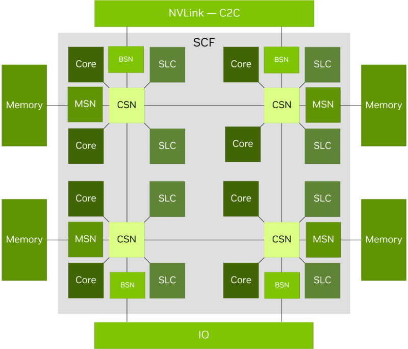
Each quadrant, in turn, is anchored by a single coherency switch node (CSN), which is responsible for routing traffic between the attached CPU cores, L3 caches, memory controllers, and I/O controllers. The CSNs are also attached to each other for when traffic needs to flow to CPU cores or memory controllers that are not part of the local cluster.
As laid out in NVIDIA’s diagram, each CSN is paired up with two clusters of CPU cores (an interesting 11 cores each), as well as two blocks of L3 cache (20.5MB/each). Finally, each CSN has a single Memory Switch Node (MSN) leading to the respective memory controller chiplet adjacent to the MSN, as well as a Bridge Switch Node (BSN) which leads to I/O. Interestingly, because Vera only has a single I/O chiplet and a single NVLink-C2C interface, both are shared by pairs of BSNs. Meanwhile this also means that a given BSN is attached or one or the other, but not both – meaning that the number of hops traffic has to go through to get from a CPU core to either of the I/O interfaces will depend on which interface it is closer to. Unlike local memory accesses, not all of the cores are equidistant from the I/O exits.
Overall, the SCF offers a massive amount of bandwidth. According to NVIDIA, there is 3.4TB/second of bandwidth along the fabric, just over 2.8x the amount of bandwidth for the complete external memory subsystem. As a result, NVIDIA says that the fabric is fast enough to allow the chip to effectively function as one large CPU despite the clustered organization, with each CPU core able to reach into other L2 cache pools or MSNs without a significant latency penalty. In other words, allowing NVIDIA to employ a distributed cache (and distributed coherency) architecture while still maintaining latencies similar to smaller monolithic designs.
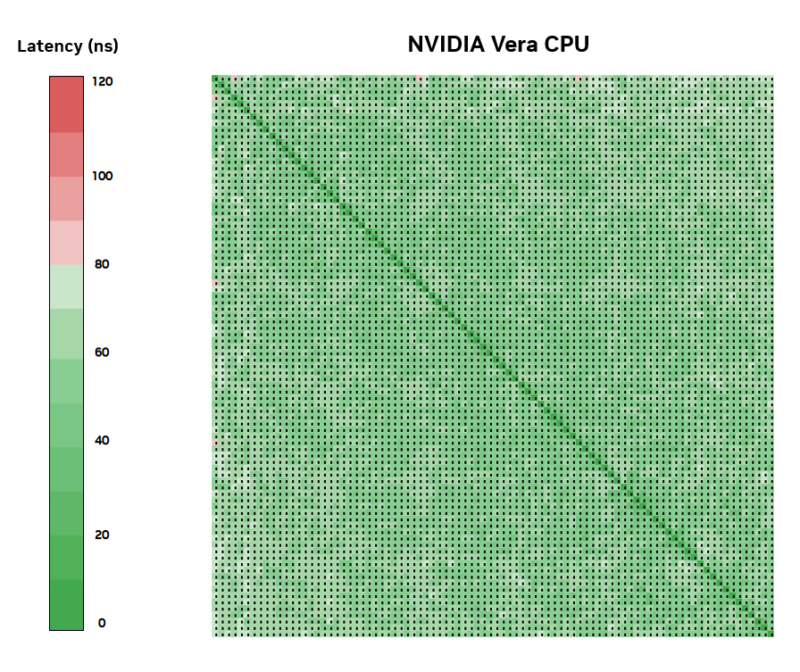
NVIDIA’s own cache latency diagram seems to back this up. While there is clearly still some benefit to staying local, we do not see the usual “block” patterns of large latency differences which we see in other CPU designs with multiple CPU clusters. Most cores seem to be able to reach another within 40ns, with only half-a-dozen core pairings exceeding 80ns. Though in some respects NVIDIA has an easier job here with Vera, as the 88 core CPU design means that there are far fewer CPU cores than the massive 128+ core designs employed by AMD and Intel.


It looks to me like someone set the colour scale on the core to core latency table so the entire table was green. Even so, the chip seems well designed for tightly coupled parallel workloads. Since AI is different than the cloud-style micro-service throughput targeted by existing processors, I think it makes sense for Nvidia to fabricate their own.
The first diagram shows only 16 lanes of PCIe 6. Surely that’s not right. How could a server CPU in 2026 ship with fewer lanes than a desktop CPU, even if they are a newer generation?
It should be noted that if Vera had been compared to the 9575F for the single-core comparisons, which you suggested would have been more appropriate, then Vera would have held a sizable advantage in the estimated SPECrate2026_int_base score. More importantly, Nvidia doesn’t seem to intend this CPU to be a general purpose CPU to go head-to-head with established processors in most data center workloads. They are targeting it for AI servers, and in particular agentic AI servers. Given how much Vera is ahead in various single core performance metrics, and considering the normal generation-on-generation IPC uplift, and that other CPU manufacturers are unlikely to have engineered a special single core monster for this upcoming generation, it seems very likely that Vera will keep an advantage for these single core performance workloads even against the coming generation of server chips. The whole reason the future CPU server TAM has recently been revised sharply upward is because of the agentic AI workload. Nvidia’s Vera CPU will live and die by how it performs against its coming-generation CPU competition in agentic AI workloads.
The microarchitecture block diagram contains multiple errors (LLM-esque). If it comes directly from nvidia (judging by the color scheme), then one has to question the accuracy of other information provided…
NVIDIA’s latest disclosure unfortunately does not go into any further detail on the branch predictor, but it does give us our first look at the instruction fetch unit it feeds, as well as the path into the 10-wide decoder. In short, Olympus’s instruction fetch unit can feed as many as 16 instructions – 64 bits each – into the decode queue. The queue can hold 48 instructions altogether, and can spit out up to 10 fused instructions to be consumed by the actual decoder.
I thought ARM ISA was 4-bytes (32-bits instruction, fixed length).
add x14,x15,x16 (4-bytes)
mul w3,w2,w4 (4-bytes)
Is that a custom ARM ISA that Nvidia is using?