
Ayar Labs TeraPHY is terrifyingly quick. At SC23, the company showed off the latest developments of its TeraPHY co-packaged optics solution and its SuperNova light source. This technology allows optics to be plugged directly into chip packages, freeing them from the confines of PCBs and long electrical traces. It is also a component of something that our readers found extremely exciting last year when we first showed it off.
Ayar Labs TeraPHY is Terrifyingly Quick with Fiber Directly Plugging into Chips
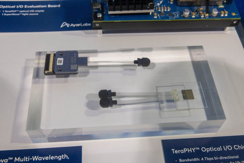
At SC23, Ayar Labs showed off its SuperNova multi-wavelength light source and its TeraPHY Optical I/O chiplet.
The SuperNova light source is important because light sources are a service item, so it seems like in the world of co-packaged optics, these are moving to pluggable modules so they can be replaced when they fail.
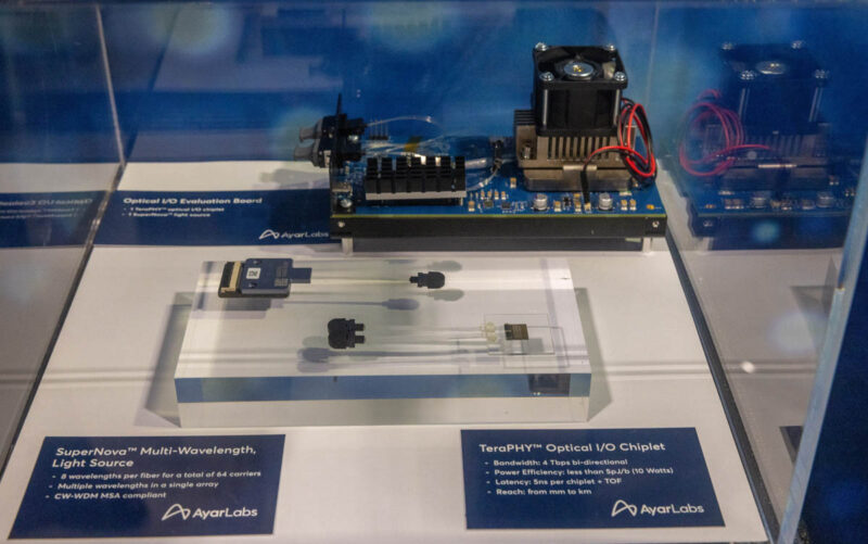
The Ayar Labs TeraPHY is an optical I/O chiplet with 4Tbps of bi-directional bandwidth at only 10W. For some sense of why this is important, put it another way, a chiplet in the same order of magnitude of power consumption as a HBM stack can provide 4Tbps of off-chip optical interconnect. Beyond just package/ component connectivity and system-to-system applications, this is one of the technologies needed to make things like pluggable high-capacity HBM packs a reality.
We took this quick photo as Ayar Labs showed us its progression from the previous gen (top) to the current gen (middle) to the next gen (bottom.)
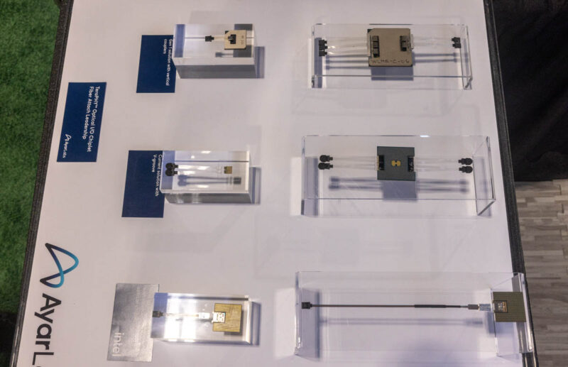
You may be wondering what that Intel logo is for at the bottom of the image above. We have already shown this at STH. It was part of Intel’s silicon photonics packaging demo at Intel Innovation 2023.
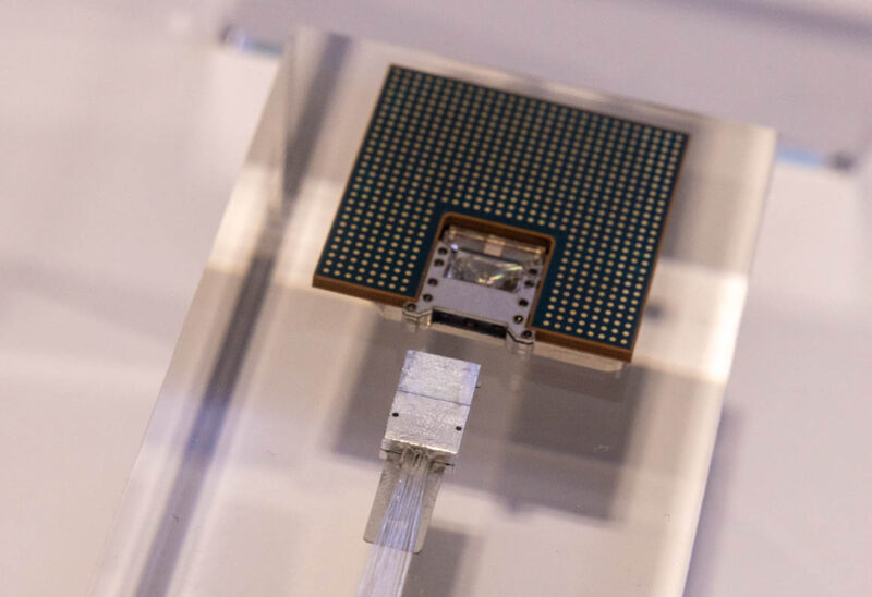
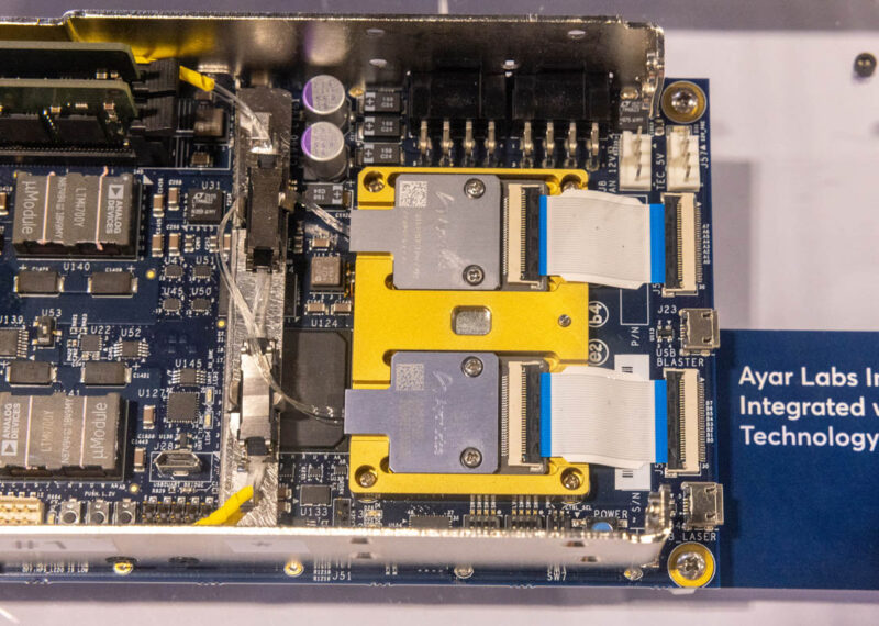
Taking a closer look, here the optical module is being inserted directly into the chip.
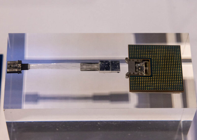
Here is another angle. The module uses a pluggable form factor so it can be replaced. There is a short run of fiber between the chip and other fiber just to ensure the physical connector is correct but also to provide a breakpoint.
Having a connector demo is cool, but seeing it work is cooler. Ayar Labs had cards with the TeraPHY and SuperNova components at the show.
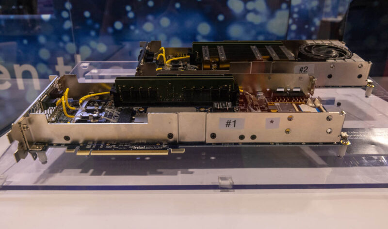
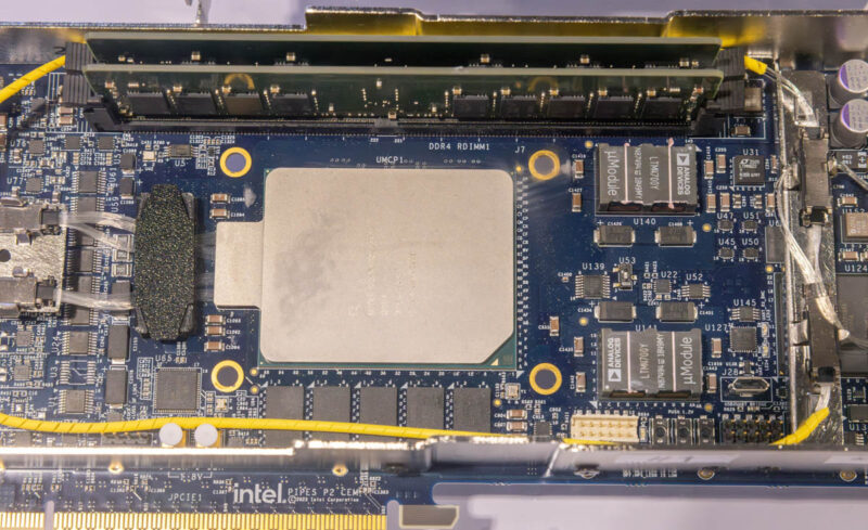
The 10nm FPGA test chip has two 4Tbps TeraPHY optical chiplets, albeit not with the pluggable connectors.
At the back of the cards, we can see the SuperNova light sources.
Ayar Labs also had two of these cards running on the show floor in a fun setup. This actually looks like a mining rig without a CPU but it is not really using PCIe for communication.
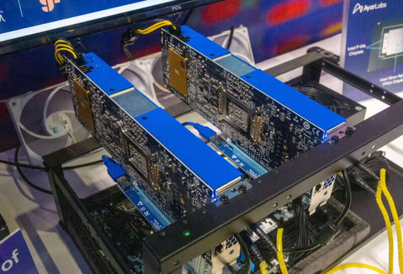
The demo showed the performance having already moved PB scale data in a few hours before we visited the demo.
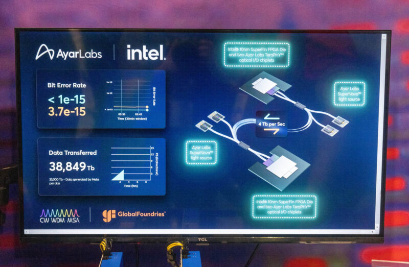
It was cool to see this working and we were told GlobalFoundries is the current fab which is why their logo is on the slide.
Final Words
This is one of those technologies that should really excite our readers. Freeing system designers from things like DDR5 slot placement on motherboards, chip-to-chip interconnects, and so forth would provide a huge benefit. Hopefully Intel can actually bring this to market, and soon.
I was chatting with Rohit, and just for some sense of how crazy this is, imagine a standard 6Gbps SATA hard drive or SSD that was able to fill the bus with data. This is like being able to directly pipe over 650 drives worth of data to the chip over optics across the data center. That is not a realistic scenario, but it is an easy way to think about the speeds we see here.
It feels like many serviceability concerns are fixed with things like pluggable connectors and pluggable light sources. Now we just need to see who is going to use this type of technology first in its high-volume chips.


I eagerly await the death of the PCIe slot.
Latency?
Bandwidth is all very fine but latency is the hard part. Does this approach allow fewer stages and interfaces, thus cutting out some delays? IB has struggled to achieve any latency improvements, and it’s becoming quite obvious with nvme interfaces. And stuff like CXL will never be interesting unless they offer improvements in latency (versus non-disaggregated).
@Mark Hahn. It would appear to do away with the entire PCIe subsystem. The interface is directly into the in-CPU inter-chiplet bus. Hard to see where you can pare any latency from that.
@Mark The latency is fantastic. There is no FEC. See slide 40 of https://old.hotchips.org/hc31/HC31_2.9_AyarLabs_20190820_HC_FINAL.pdf (2019). In the first TeraPHY chiplets, latency is <10ns + time-of-flight (5 ns/m) for chiplet-IO-…-chiplet-IO (electrical-…-electrical) for an energy of <5 pJ/b. When I heard this back in 2019, I knew this kind of interconnect is inevitable, once you boil the test and assembly oceans.
Comments are closed.