
For this year’s Integrated Systems Europe trade show, AMD is unveiling an upgraded lineup of its Kintex mid-range FPGAs. Dubbed the Kintex UltraScale+ Gen 2 family, this latest iteration of the Kintex family is designed to modernize the FPGAs, bringing support for newer and faster memory, I/O, and cryptography technologies. As with the existing (Gen 1) Kintex UltraScale+ parts, AMD is planning on offering the FPGAs over the long term, with availability through at least 2045.
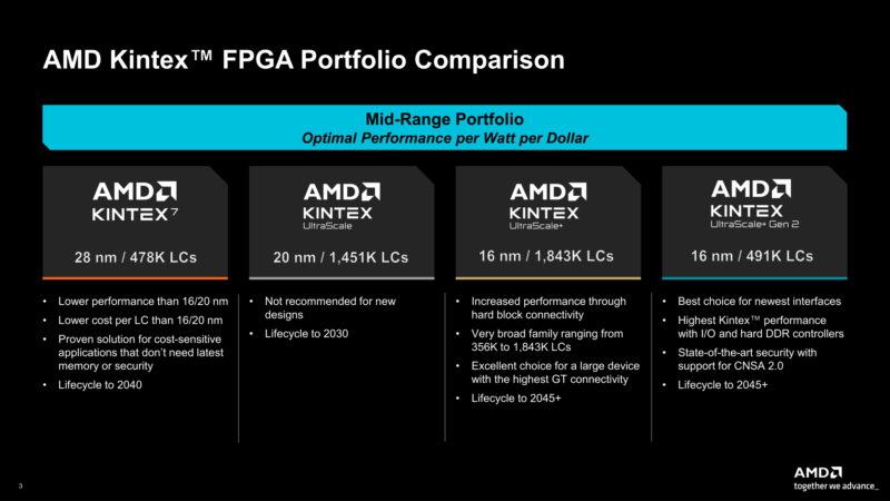
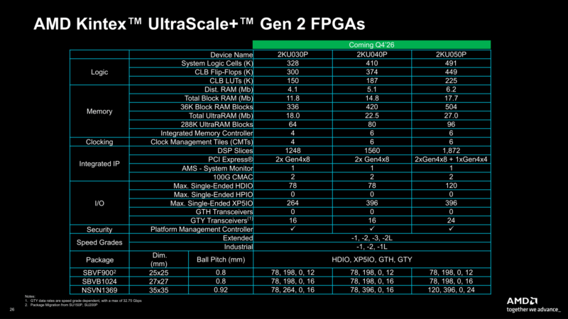
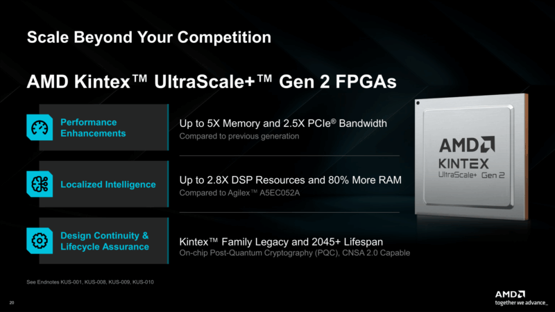
At a high level, the new Kintex UltraScale+ Gen 2 parts are intended to augment the lower-half of AMD’s existing Kintex UltraScale+ SoC family. Altogether there are 3 planned versions of the Gen 2 chips, with the largest topping out at 491,000 logic cells. With both the original and Gen 2 chips intended to be available out to the same 2045+ timeframe, the Gen 2 chips are not so much a replacement for the previous chips as they are another option for customers who need more (and more modern) I/O resources for a given FPGA compute performance level.
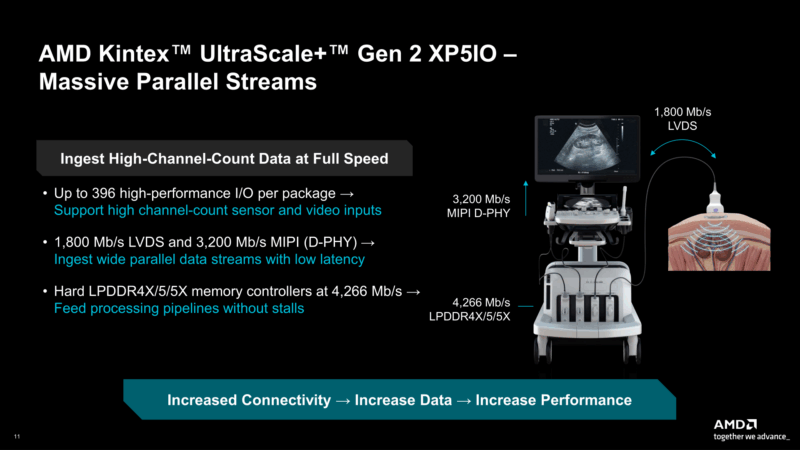
Compared to the original parts, the biggest upgrade here are the memory controllers, which AMD is significantly bulking up. Whereas the comparable gen 1 parts all feature a single hard block 64-bit DDR4 memory controller, the Gen 2 chips increase this to either 128-bits (4×32-bit hard blocks) or 192-bits (6×32-bit hard blocks) of LPDDR4X/5/5X depending on the SKU. As a result, the Gen 2 chips offer multiple times the memory bandwidth of the original chips, boosting bandwidth both via the 2-3x larger memory bus, and being able to run at 4266Mbps/pin, versus DDR4’s more pokey 2677Mbps/pin.
The memory technology update also serves to help future-proof the FPGAs over the long window that AMD wants to offer them. DDR4 production is already in decline, whereas LPDDR – and particularly LPDDR5X – is going to be readily available much farther in to the future. So although the Gen 2 chips are not especially taking advantage of the higher bandwidth potential of LPDDR5(X), being able to interface with the newer memory is still a big deal on the time scale that AMD is planning for.
Speaking of memory, the Gen 2 chips are also embedding a larger amount of SRAM than their predecessors. The top Gen 2 chip will come with a combined 51Mbit of SRAM, versus 41Mbit on its predecessor, giving them both more bandwidth to external memory, and more internal memory for buffering resources as well.
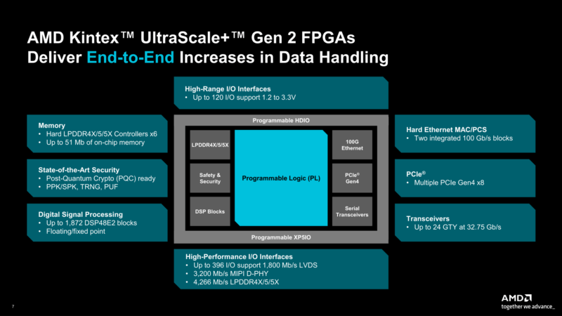
Moving on, the other big hardware capacity upgrade with the Gen 2 chips will be in terms of I/O. The top-end SKU is bumping the total number of 32.75Gb/second GTY transceivers from 16 to 24. Complementing that, the on-chip PCIe blocks have been upgraded from PCIe Gen3 to PCIe Gen4, allowing for 2-2.5x as much PCIe bandwidth as on the previous chips. In this case AMD is using PCIe Gen4 x8 controllers, with two or three of those blocks built in to the FPGA depending on the SKU.
Otherwise, customers are free to use the rest of the additional GTY transceivers (and XP5IO pins) as they see fit. AMD for their part seems to be banking hard on 100Gb Ethernet, as evidenced by the fact that the Gen 2 chips integrate two hard blocks for 100Gb MACs – twice as many as before.
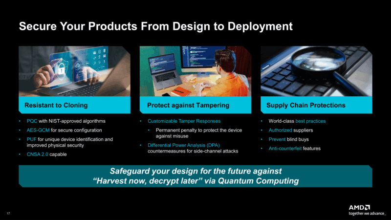
The final big-ticket hardware improvement for the Gen 2 chips comes with its cryptography support. AMD has added support for multiple post-quantum cryptography cyphers, including the US National Security Agency’s Commercial National Security Algorithm Suite 2.0 (CNSA 2.0), which mandates the algorithms used in US national security systems. And government requirements aside, AMD sees PQC as a further tool to harden the Gen 2 chips so that they can reliably serve out to 2045 by limiting the ability for attackers to tamper with or clone the circuit designs uploaded to the FPGAs.
For the rest of the hardware specs, the Gen 2 chips are relatively similar to their predecessors. The top-end chip packs 491K logic cells and 1872 DSP slices, with clockspeeds ranging from 600MHz to 1066MHz, which should result in relatively similar performance. Notably, the new chips are not being fabbed on a newer process node either – AMD is sticking with tried-and-true 16nm FinFET for this – so there are not any major gains to be had from manufacturing improvements. Rather, all of these additional features come from building larger and more complex chips, which is undoubtedly part of the reason why AMD did not bulk up on compute performance as well.
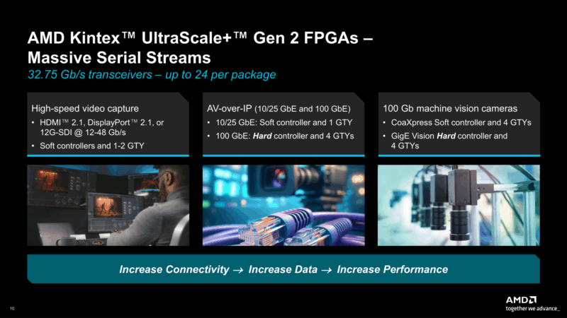
The target market for the new chips, in turn, is going to include the healthcare, robotics, broadcast, and machine vision markets. It is a fairly broad range, essentially covering any user base who needs something with the expanded I/O and memory capabilities of the Gen 2 chips to handle more concurrent/multi-steam workloads – but does not need the compute performance afforded by the larger gen 1 chips.

Wrapping things up, with today’s announcement being timed to a trade show, AMD is announcing the Kintex UltraScale+ Gen 2 chips well ahead of product availability. The company will be sampling the chips in Q4 of 2026, and full-scale production will kick off in the first half of 2027. Which with the 2045+ lifecycle for the chips, means AMD will be offering them for at least 18 years after they launch.


With all those 32Gb/s transceivers onboard, why do they have just PCIe4 and not PCIe5 ?
Looks like a big oversight to me.