

At Hot Chips 2026, Samsung is presenting Evolving HBM Base Die, a look at how the company wants to turn the base die of high-bandwidth memory into something far more capable than a passive interposer. We are covering this talk live, so please excuse any typos.
Samsung Evolving HBM Base Die at Hot Chips 2026
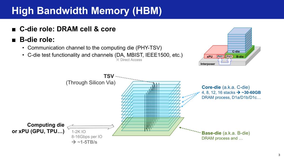
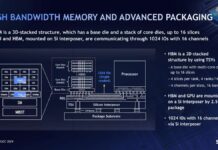
HBM splits its work between the DRAM core dies stacked above and the base die underneath. Samsung calls the stacked memory layers C-dies, while the base die, or B-die, carries the PHY and through-silicon vias that form the communication channel to the compute die. Four, eight, twelve, or sixteen C-die stacks land on that base die. If you need a visual, here is the diagram.
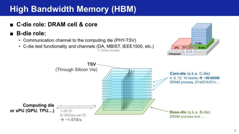
HBM bandwidth and capacity have climbed steadily since the first generation. Samsung’s historical figures trace maximum capacity from roughly 1 GB and 1 TB/s in the original HBM through to an HBM5 generation that pushes past 60GB and 6 TB/s. Rising bandwidth, more than capacity alone, keeps forcing fundamental changes in the base die.
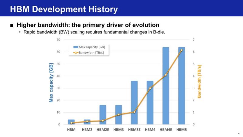
Several limits throttle how fast HBM bandwidth can grow. Samsung points to through-silicon via counts and pitch on both the C-die stack and the base die, along with the I/O count and speed of the PHY embedded in the B-die. Here are TSV and DQ counts against pitch and area across generations to show where the pressure builds.
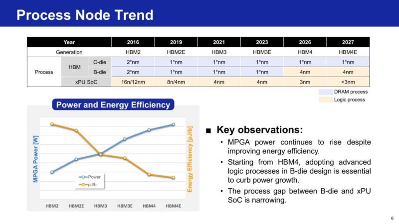
Process technology for the C-die stays on DRAM-class nodes, but the base die has started to move. Samsung’s trend table shows the B-die shifting from older logic process toward 4nm starting with HBM4, narrowing the gap to the XPU SoC. Even as energy efficiency improves, MPGA power keeps rising, which is why Samsung says advanced logic in the B-die becomes essential from HBM4 onward.
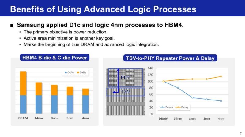
Samsung applied its D1c DRAM process and logic 4nm to HBM4, with power reduction as the primary goal. Active area minimization matters too, and this work marks the beginning of true DRAM and advanced logic integration. Samsung’s trace across process nodes shows both TSV-to-PHY repeater power and delay dropping as the logic node advances.
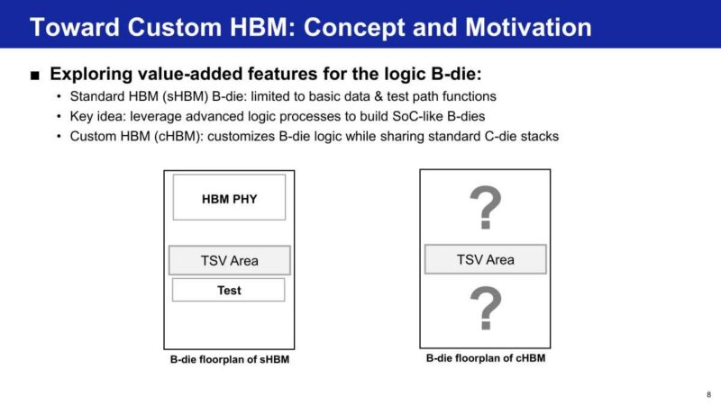
Standard HBM, which Samsung calls sHBM, keeps the B-die boxed to basic data and test-path functions. Custom HBM, or cHBM, instead uses the advanced logic process to build a more SoC-like base die while still sharing standard C-die stacks. We looked at custom HBM previously from even non-memory vendors like Marvell in the past.
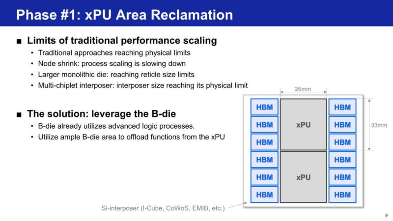
Traditional scaling is hitting physical limits. Node shrink is slowing, monolithic dies are near reticle limits, and multi-chiplet interposers are hitting size limits. Samsung’s answer is to use the base die, which already runs advanced logic, to offload some functions from the XPU onto the B-die.
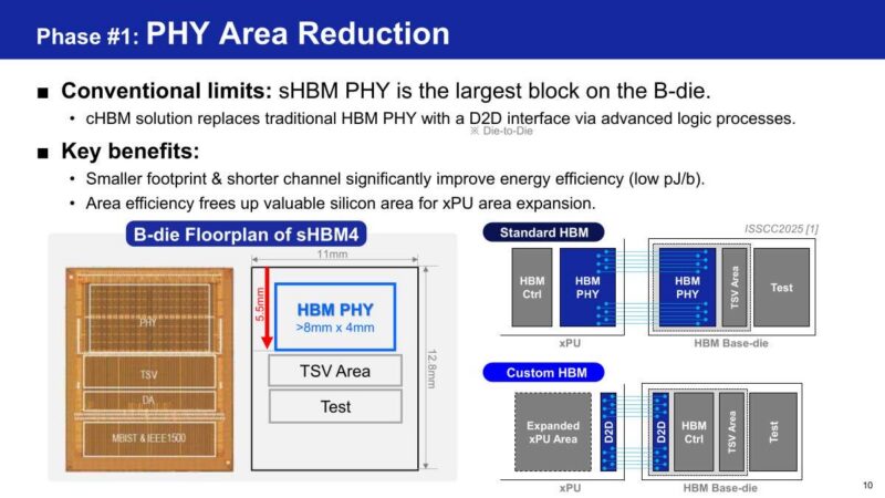
On today’s standard HBM, the PHY is the largest block on the base die. Samsung replaces the traditional HBM PHY with a die-to-die interface built on advanced logic, shrinking the footprint while also shortening the channel for better energy efficiency. This freed silicon becomes room for XPU area expansion, as the floorplan comparisons show.
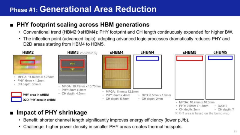
Across HBM2 through sHBM4, PHY footprint and channel depth kept expanding to feed higher bandwidth. Advanced logic sharply trims PHY and D2D area from HBM4 into HBM5 by packing more power into a smaller area for the PHY. Shorter channels cut energy per bit, but packing more power into a smaller PHY raises power density and creates thermal hotspots.
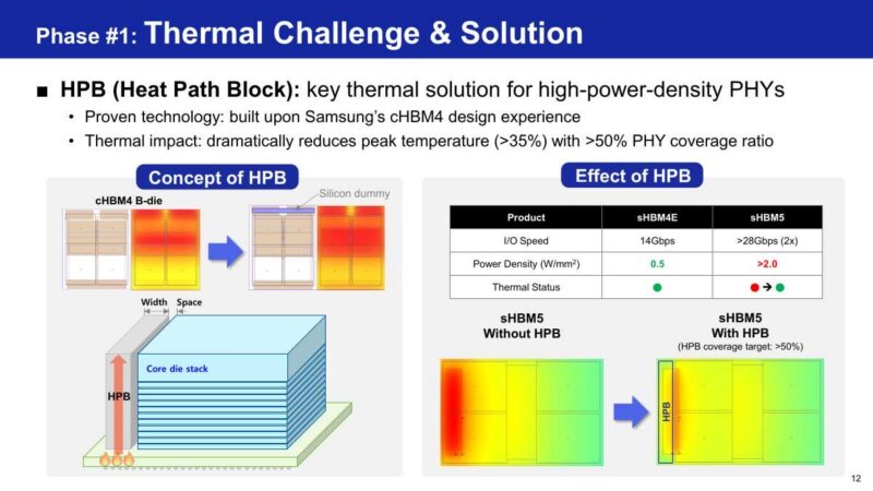
That thermal pressure gets its own solution. Samsung proposes a Heat Path Block, or HPB, built on its cHBM4 design experience. With PHY coverage above a target of 50 percent, peak temperature drops by more than 35 percent, which Samsung needs as I/O speed roughly doubles from sHBM4E to sHBM5 and power density climbs from 0.5 to over 2.0 W/mm2.
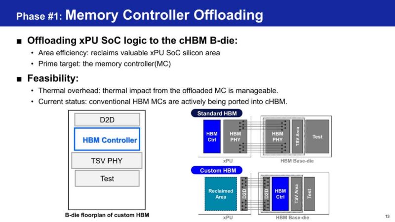
Once the base die has room, Samsung starts moving XPU logic onto it. Its prime target is the memory controller. Moving the MC to the B-die reclaims valuable XPU silicon, and Samsung says the thermal impact is manageable, with conventional HBM memory controllers already actively being ported into cHBM.
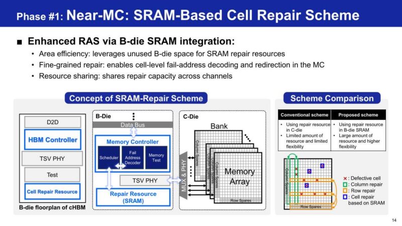
Putting SRAM on the base die also improves reliability. Samsung’s SRAM-based cell repair scheme uses unused B-die space to decode and redirect failed-cell addresses with fine granularity, sharing repair capacity across channels. Compared with conventional repair that relies on limited spare resources in the C-die, this approach provides larger, more flexible repair resources in the B-die.
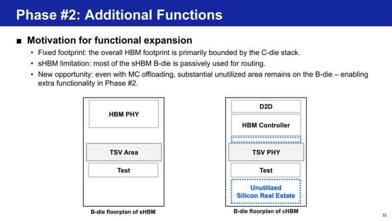
Phase one leaves substantial silicon on the table. Since the overall HBM footprint is mostly bounded by the C-die stack, and most of the sHBM base die is passive routing, Samsung sees room even after the memory controller moves off. That unutilized B-die real estate becomes the basis for phase two’s expanded function set.
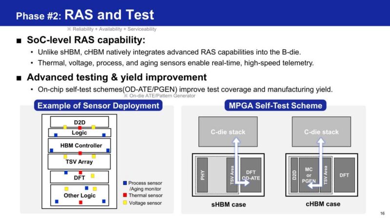
Custom HBM brings SoC-level RAS into the base die, something standard HBM lacks. Samsung integrates thermal, voltage, process, and aging sensors for real-time telemetry, along with on-chip self-test schemes such as on-die ATE and pattern generators, to improve test coverage and yield. This sensor-and-self-test deployment is what distinguishes the cHBM case from the sHBM case.
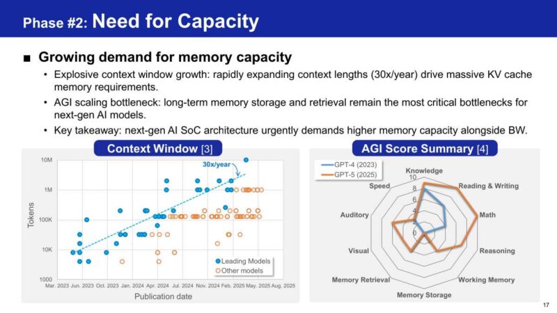
Capacity demand is growing as fast as bandwidth. Samsung points to context windows expanding around 30x per year, which drives massive KV cache memory requirements, and calls long-term memory storage and retrieval a critical bottleneck for next-gen AI models. That points next-gen AI SoCs toward higher capacity, not just higher bandwidth.
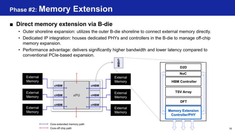
One way to add capacity is to hang external memory directly off the base die. Samsung uses the outer shoreline of the B-die to connect external memory through dedicated PHYs and controllers integrated on the die. This delivers higher bandwidth and lower latency than conventional PCIe-based expansion.
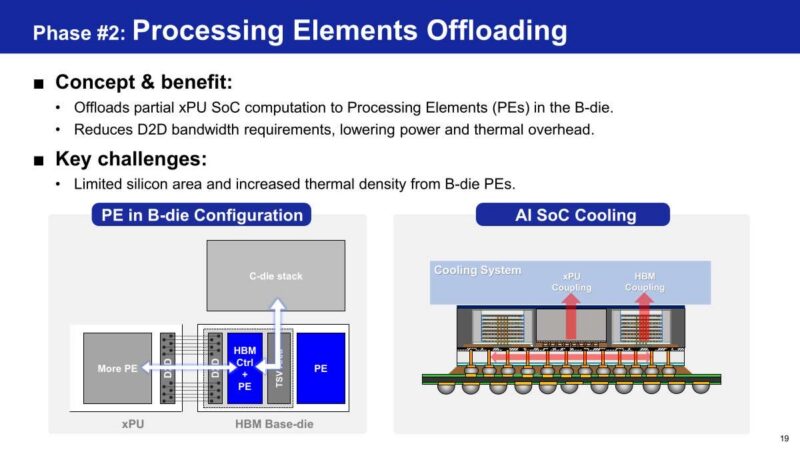
Samsung also sees room to offload computation onto the B-die. Processing elements in the base die can take partial work from the XPU SoC, cutting die-to-die bandwidth demand and lowering power and thermal overhead. Limited silicon area and rising thermal density from those PEs are the key challenges.
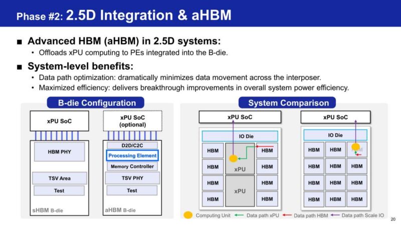
With processing elements integrated into the base die, Samsung takes a step further into 2.5D systems. Advanced HBM, or aHBM, offloads XPU computing to those PEs, minimizing data movement across the interposer. Samsung describes the resulting power efficiency gains as a breakthrough at the system level.
Phase three moves beyond the interposer entirely. Samsung argues the industry is shifting toward tightly coupled AI memory and that maximizing tokens per second within strict power limits is the challenge for inference. zHBM is the answer, a true 3D vertical integration of the XPU and the C-die stack that removes the 2.5D interposer.
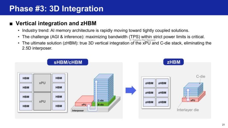
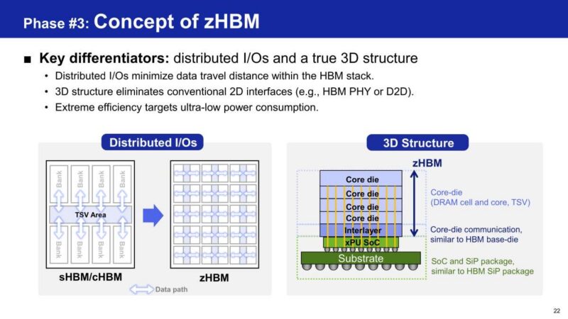
zHBM changes the physical story of HBM. Distributed I/Os shorten the distance data travels inside the stack, and the true 3D structure eliminates the conventional 2D interfaces such as the HBM PHY or D2D. Samsung targets ultra-low power consumption with this arrangement.
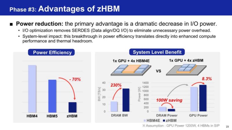
Power is the headline advantage for zHBM. Removing SERDES and the data-alignment overhead cuts I/O power dramatically, and Samsung’s system-level estimate shows this translating into compute and thermal headroom. In one example, four zHBM stacks in a SiP, alongside a 1200 W GPU, deliver a significant bandwidth increase while saving around 100 W.
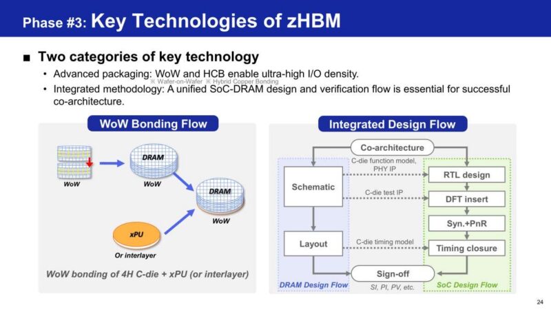
Delivering zHBM leans on two technology pillars. Wafer-on-wafer bonding and hybrid copper bonding enable the ultra-high I/O density, and Samsung stresses that a unified SoC and DRAM design and verification flow is essential for the co-architecture. This figure lays out the WoW bonding flow alongside the integrated design flow that co-develops the DRAM C-die and XPU.
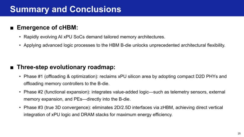
Samsung closes by framing the roadmap. Applying advanced logic to the base die unlocks architectural flexibility that offloads and optimizes in phase one, expands functions in phase two, and converges to true 3D integration with zHBM in phase three. That three-phase path, from reclaiming the XPU area to eliminating the interposer, is what Samsung argues will move the HBM base-die design forward.
Taken together, these figures show how Samsung is approaching the evolving HBM base die.
Final Words
This base die is becoming a co-processor rather than a passive interposer, which changes where memory and logic are designed within an AI system. Moving the memory controller, and eventually processing elements, into HBM gives accelerator vendors a new home for part of their silicon. zHBM, however far off it is, points the industry toward stacking compute directly on DRAM and removing the interposer. System architects should watch this shift closely as the next HBM generations land. What a neat Hot Chips 2026 talk.
We have a full recap on the Substack, including where all of these pieces ranked in terms of popularity:

Where I see b-die headed is becoming wider to encompass multiple stacks of c-dies for both capacity and performance reasons. The next step after that would be to tile xPU around each b-die in a checkerboard like fashion: there are for external links going north, south, east and west. The b-die would encompass the memory controller function for all the neighboring xPU dies, including local coherency with respect to memory accesses to the c-die stacks. Bandwidth would increase as the b-die would be handling four times as many connections, though the real bottleneck could shift between the TSV between the b-die and c-dies. Since the HBM spec mostly dictates the link between the b-die and the xPU, there is room to implement more proprietary TSV interfaces.
The idea of putting external memory controllers on to the b-die is a cleaver means of increasing capacities. However on a physical system design perspective, where is that external memory going to live? Various AI accelerators are packed pretty tightly together today to enjoy lower latency and hyper fast interfaces between each other over the motherboard. Adding space between them for 8 CAMM modules (four from each socket) would impact that performance. At this juncture, moving to copackaged optics for the local coherent links would resolve that issue and permit each xPU to be come on its own daughterboard. This is a good idea but it has ramifications else where in the system design to be useful.
zHBM is going to be interesting to watch as it effectively moves the b-die functionality onto the xPU die. While certainly faster and conceptually lower power, it also does have the negative effect of not being able to put as much xPU logic in the system. This is a reduction in compute capabilities of the xPU dies. Given that memory bandwidth and capacity are often the limiting factors in current designs, perhaps scaling back compute a little bit is the appropriate trade off. However, I suspect that the checkerboard topology I described above would be a better design to scale. There is also a cost factor as newer nodes are extremely expensive. With a checkerboard topology, the b-die would not need to be manufactured on a leading edge node. Similarly, leading edge nodes have their maximum die area decreasing which could prevent a four stack design on top of the xPU.
AMD has already hinted at adopting zHBM directly onto some of their products in the future. Earlier roadmaps for their GPUs put this as a ‘post HBM’ time frame with directly stacked memory.
Lastly one thing not touched on here is that the density of SRAM on leading edge nodes is going to be eclipsing that of DRAM soon. While SRAM is not scaling in density like it used to, it still is at the leading edge. DRAM on the other hand hasn’t been able to break past 10 nm due to how DRAM capacitors are designed. Thus a 14A process might be able to put an entire multi-transistor SRAM into the same area as that DRAM capacitor. This would permit HBM to increase clocks and capacity as newer nodes come online, though in a very, very expensive manner. Given that AI designs are still operating in a fashion that money is no object, this could be under consideration.