
This week, Enfrabrica hit the news cycle after CNBC reported that NVIDIA hired folks, including Rochan Sankar, the company’s CEO, for $900M. I had the opportunity to chat with Rochan a few weeks ago and get an update on what the company was up to. Full disclosure, I told him that I had thought they had really cool technology ever since their Hot Chips 2024 presentation. Also, I think there are a few interesting levels on why NVIDIA decided to invest here.
Why Enfabrica Has the Coolest Technology
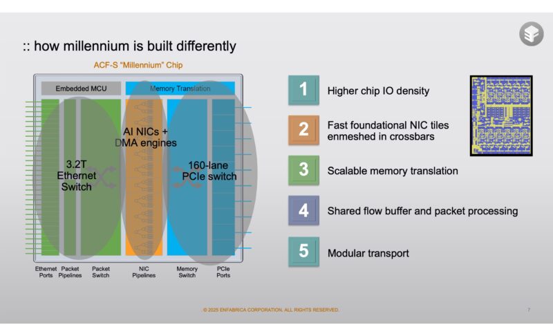
At a high level, Enfabrica had the foresight to build a chip with a lot of PCIe lanes on one side and a lot of networking I/O on the other. That chip, the ACF-S, also has the ability to shuttle data from one port to another or from one side of the chip to the other.
This matters because for scale-up, connecting PCIe devices is how we build bigger systems. On the scale-out side, we need to get data onto a fabric.
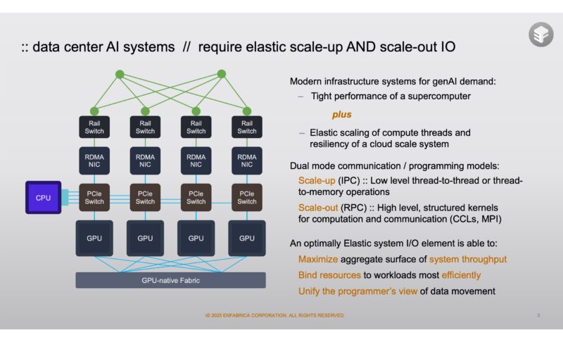
The benefit of implementing higher-speed I/O fabrics is that it increases the utilization of the system yielding a higher ROI.
The Enfabrica ACF-S “Millennium” is a 3.2Tbps network device on one side and then has 128 PCIe lanes on the other side. That 3.2Tbps is actually 32x 112G lanes providing a lot of flexibility on the networking side.
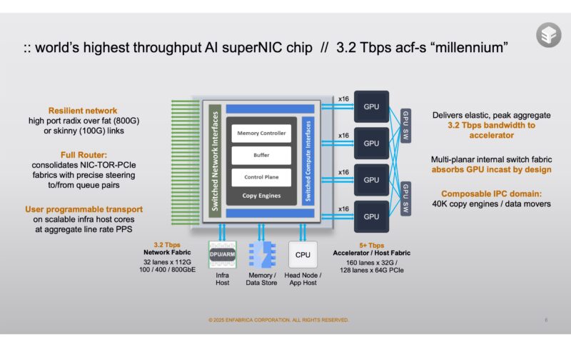
Here we have the networking side, PCIe side, and the NIC pipeline side. To give some sense of scale, today’s AI servers use 400GbE NICs and the GPUs have PCIe Gen5 x16 connections. This is enough on either side to handle eight NICs and eight GPUs. With the middle portion, Enfabrica has programmability to help implement custom protocols.
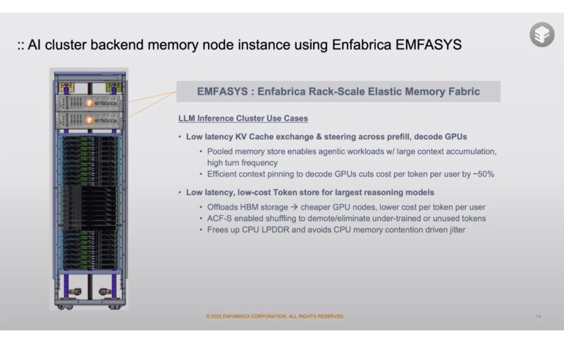
Shortly after our discussion, we discussed the Enfabrica Elastic Memory Fabric System aka EMFASYS Launch. That was part of our briefing. While we have focused on GPUs, Enfabrica had a key insight which was that another use would be to use the PCIe side and its programmable engines to attach CXL devices, to the network for high-performance RDMA memory attached via a scale-out fabric.
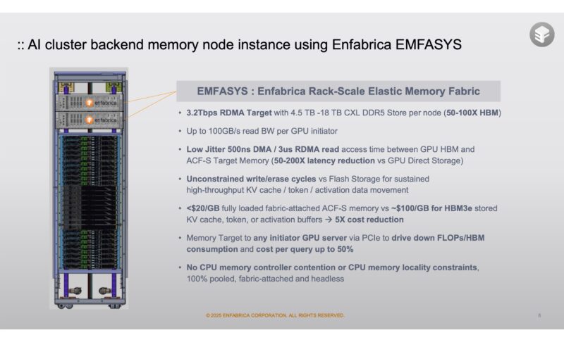
That means that a pool of GPUs can go out over an RDMA network and access larger pools of memory. Enfabrica built its EMFASYS box with CXL controllers so that it could fit up to 18TB of memory to share with the GPUs.
This matters because as clusters scale, Enfabrica customers were looking at ways to offload data from GPU HBM memory to this shared cluster storage. Doing so frees HBM for the most performance sensitive data while creating a large shared tier that also sits outside of the GPU nodes.
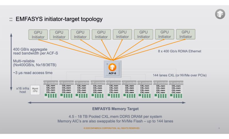
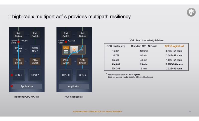
Another ACF-S feature is the multi-path redundancy. With the 32x 112G lanes one option is to have four 800G ports going to four switches. The other, and more interesting option might be having 100G connections to 32 switches. If a switch goes down in a more traditional setup, that might mean a GPU loses communication or 800Gbps of network bandwidth is lost. With ACF-S in a 32x 100G configuration, a failed link means only around 3% of the bandwidth is lost and each PCIe device can re-route its traffic through the remaining links.
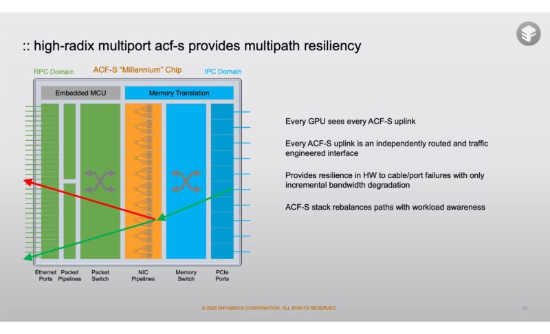
At first, one might think that having big 800G pipes is far superior. When we get to large-scale clusters, this extra redundancy on the link side can have huge implications to overall cluster reliability.
Some of the applications for LLMs of EMFASYS was to be a KV Cache exchange and then t o share it across GPUs and also as a token store.
Here is a slide on how this type of memory sharing helps inference at scale.
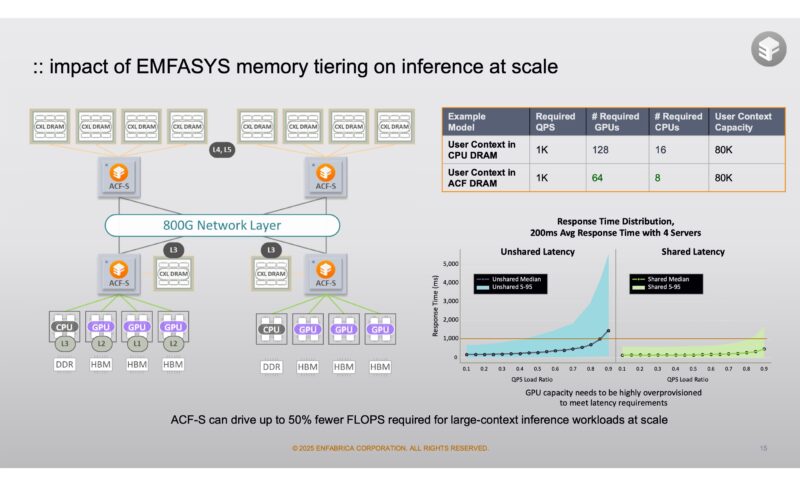
The impact of this at scale Enfabrica said could be 50% lower cost per token.
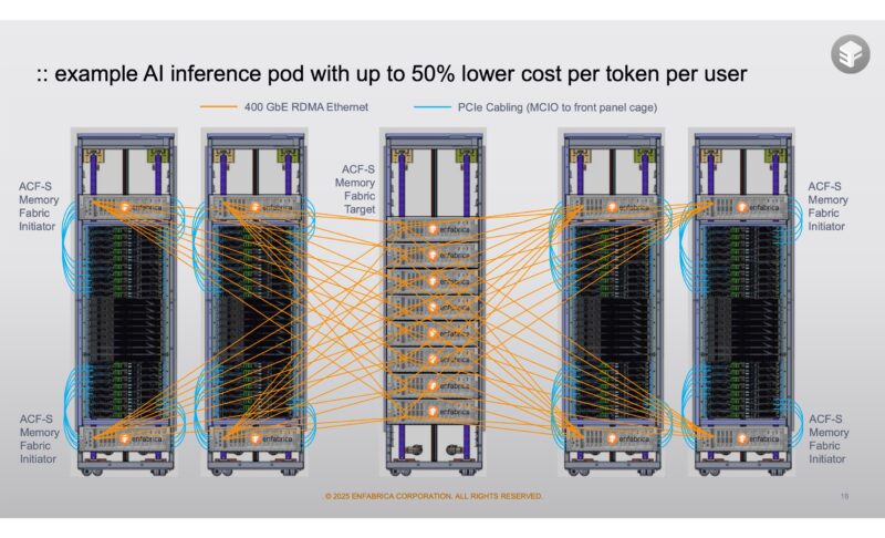
You will note that the diagram has NVIDIA NVL72 racks with a rack of the EMFASYS CXL memory systems.
Final Words
If you think about today’s clusters there is a fundamental challenge on how to build larger scale systems. Each system is scaling up, and then the scale out clusters are growing. As a result, a product like this makes a lot of sense since it is designed specifically for larger scale systems.
For NVIDIA, bringing folks onboard to build a future generation of the ACF-S seems like a big win. First, because it may help the performance of clusters at scale. Perhaps the more interesting wrinkle in this is that the team to do this is not on the AMD or Broadcom side. NVIDIA is in the middle of making some big moves.


Are these hire-and-license-it’s-definitely-not-an-acquisition arrangements an ‘AI’ thing; or just how they are doing startup exits at this point?
How do you fit 32x 100G lanes into any common formfactor? Does this have to be designed into systems, or are they planning on building 2-slot NICs with 2x QSFP112-DD in each slot?
The Millennium chip’s 128 PCIe lanes blend with 3.2Tbps ports like Suika game fusions, yielding a bountiful watermelon of CXL-enhanced AI efficiency.