
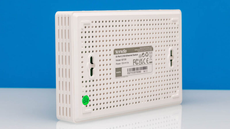
The Tenda SE108 is an 8-port fanless 2.5GbE switch. It is also extremely similar to the BrosTrend S3 switch we reviewed. Still, we wanted to keep the refresh of our The Ultimate Cheap Fanless 2.5GbE Switch Buyers Guide going and wanted to validate that this was similar to the BrosTrend. We bought one to test out, even though it was $11 more than the BrosTrend when we did.
Here is an Amazon Affiliate link to the Tenda SE108, and another Affiliate link to the BrosTrend S3.
Tenda SE108 Hardware Overview
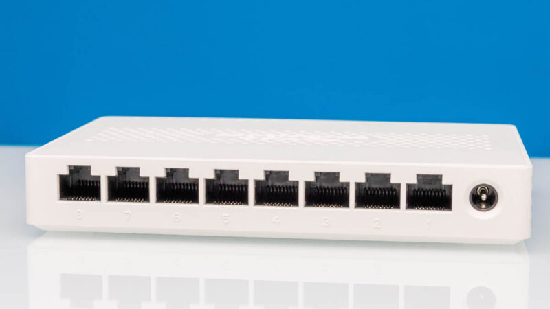
The front of the Tenda SE108 is where all of the ports are located.
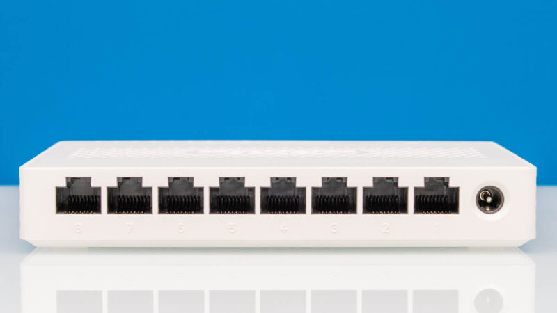
There are eight 2.5GbE ports here, versus just five on the Tenda SE105 and BrosTrend S2.
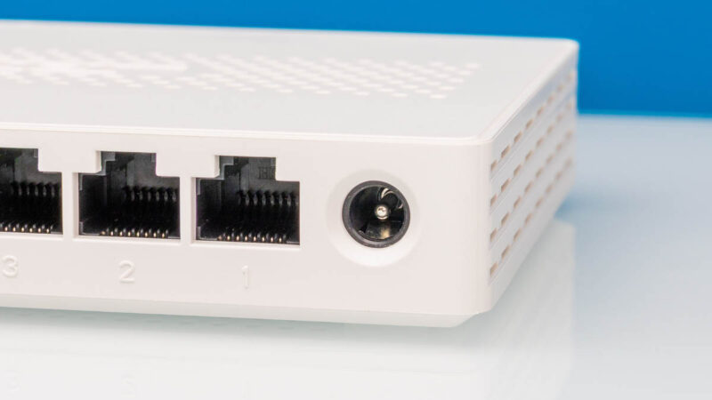
There is also the 12V DC input jack on the front faceplate.
On the top and side, we get vents. The top also has the LED status indicators.
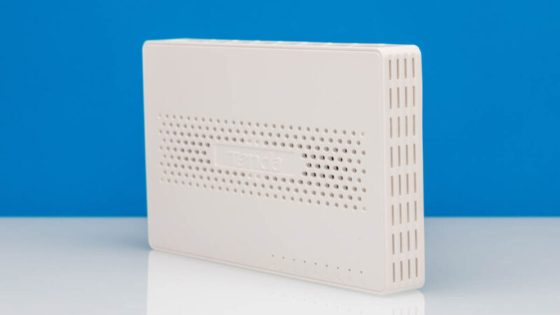
On the other side and bottom, there are more vents. There are also mounting points on the bottom. Again, like the BrosTrend S3 and the 5-port BrosTrend/ Tenda models, we get plastic instead of rubber feet.
Opening the switch, we get something slightly different, or at least we thought so at first. There was a metal part stuck on the bottom, which was not present on the 5-port version.
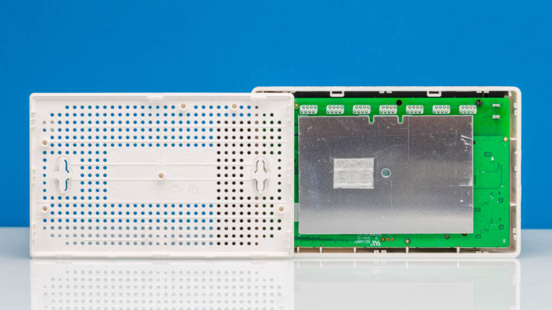
This is a backside cooler for the switch chip.
We thought this was different from the BrosTrend S3 until we realized it was the one that came off the bottom cover. On the Tenda, the double-sided tape did not hold, whereas it did on the BrosTrend.
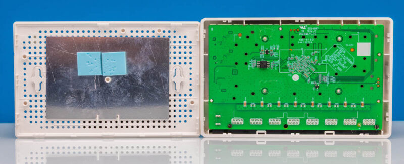
This bottom side cooler is also one of the major differences between this Tenda SE108 8-port model and the SE105 5-port model.
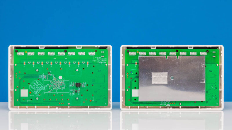
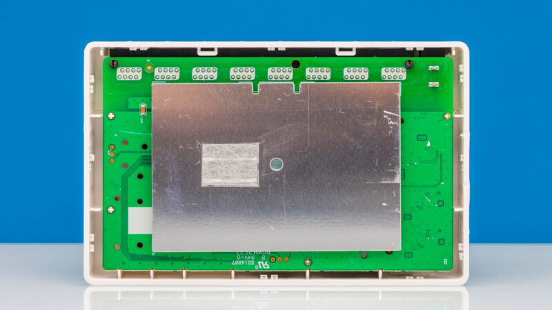
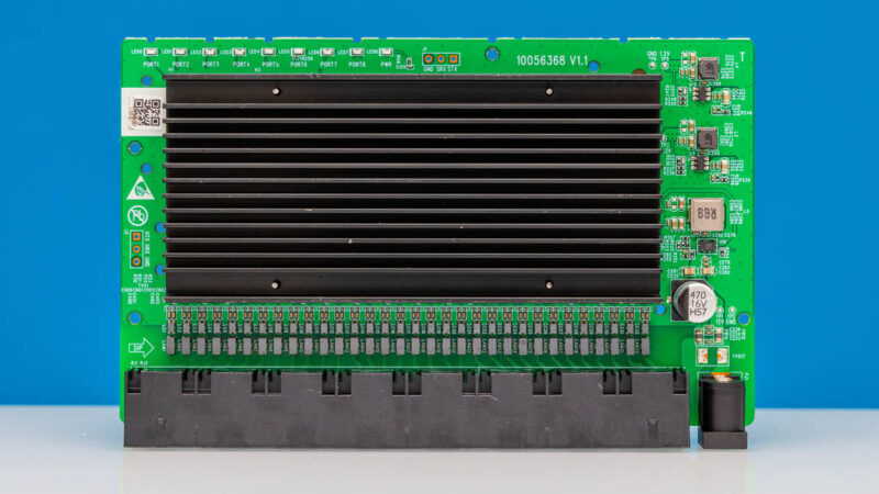
On the top, we get the larger heatsink we see on the 8-port models and all of the 2.5GbE ports placed. The switch PCB has the same 10056368 V1.1 we saw on the BrosTrend and even the 5-port models.
It seems like the 8-port models just add the extra ports and then increase the cooling capacity.
Next, let us power the switch on and see how it works.


I’d be curious what the peak power consumption was, with all ports lit up and traffic flowing. 1.3 + 8 * 0.3 = 3.7W? more?
I’d also be interested to see somewhat more precise measurements on the DC side of the power supply, since the wall warts that come with these products are… suspect.
Not something that would need to be done for every model, but maybe one per chipset for these common chips when they’re all just using the reference design.
I agree.
It would also be very interesting to know the power consumption of each of the switches using a laboratory power supply. That way we would know the real consumption of each of the chipsets discarding the quality of the power supply provided.
I also think it would be very interesting if they tested the behavior of unmanaged switches with frames with VLAN tags. Some switches block these frames while others let them pass through transparently and unaltered.
For the power consumption measurements, it would be relevant what kind of “Energy Efficient Ethernet” was active. Basically: Does the switch offer it, at which speeds and was it successfully negotiated.
The per port power consumption hugely differs depending on this.
And I agree with the previous posters – measuring at the DC side is also relevant.
I noticed: When fully activating EEE and supplying the switch with a high quality 5v power supply, the advantages of the MaxLinear platform are gone.
Nothing in these switches needs 12V – it just makes it more inefficient when converting down from 12V.
It’s just a normal switch branded has tenda . Next and. Netis does the same thing
I am still skeptical as I dont have good experience with tenda. I didnt find them reliable, although very reasonable pricing but still would consider netgear or even tplink.