MikroTik CRS418-8P-8G-2S+RM Internal Hardware Overview
Inside, we can see a fairly neat layout. At the back of the switch, we have the power inputs and fans. In front of the switch, we have the switch PCB and the power supplies.
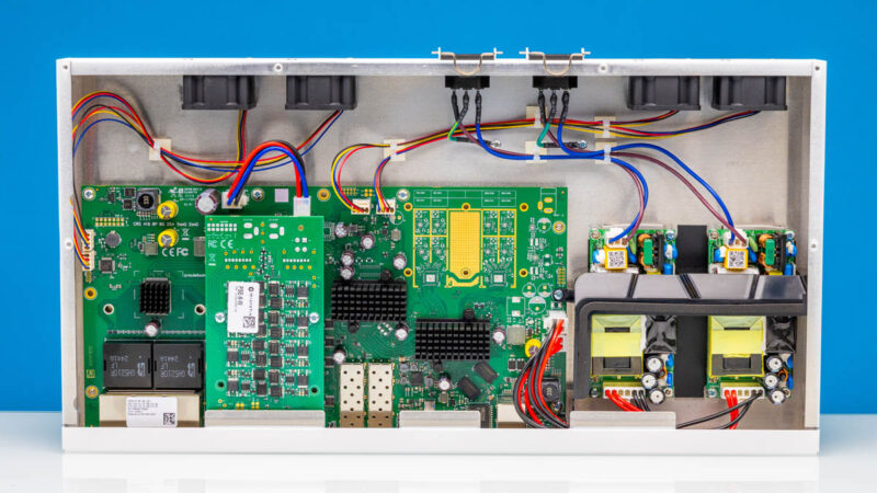
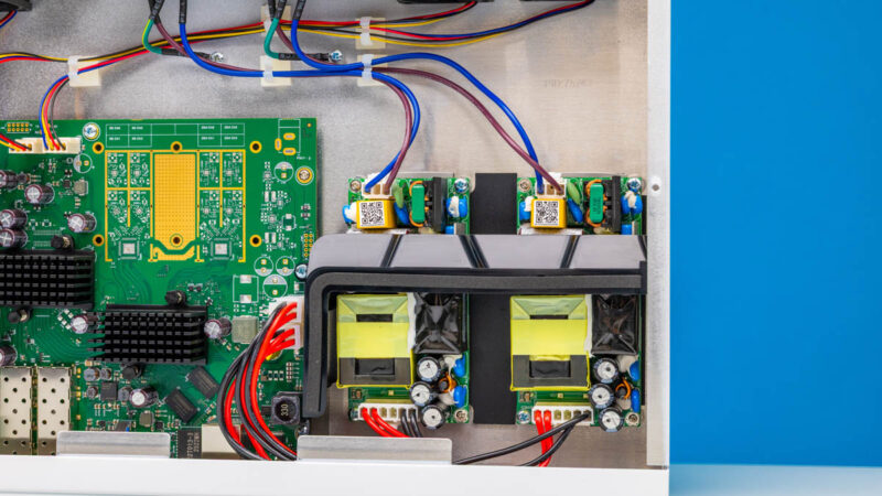
The 250W power supplies are actually in the front of the chassis. These are not hot-swappable, but a replacement part, TN19-0250-55, is available. We like that MikroTik is making the part available, even at a $69 or so price, so that if you were concerned with power supply failures, you could purchase a spare.
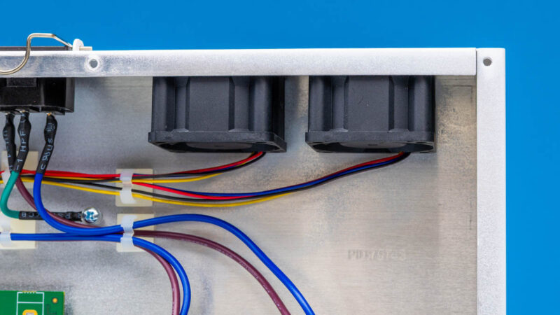
Inside, we also have the fans. Unlike some of MikroTik’s higher-end switches, these are not hot swappable.
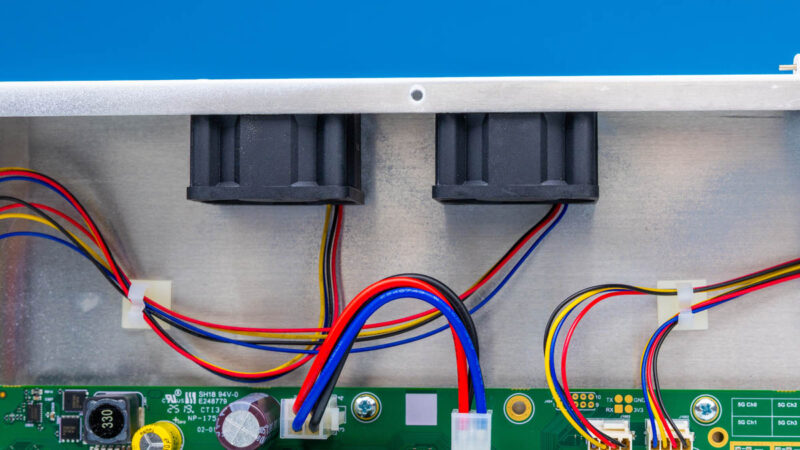
There are four fans inside, all connected via 4-pin PWM headers. We know some readers will think about fan swaps, but these are very quiet in practice.
As we will get to in our power and noise section, the impact of having four fans is that the setup is relatively quiet. It seems like MikroTik added more fans, and therefore cost, in order to ensure that the setup remained quieter. That is a great trade-off in our book. Also, having more fans means that if one fails, there is still airflow through the chassis. That is always a worry on single fan switches and routers.
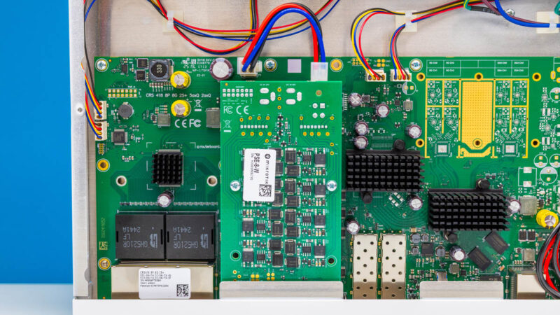
On the main switch PCB, you can see the placement spot for the WiFi radios that are unpopulated in this switch.
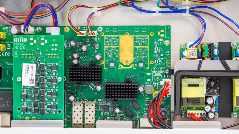
Often, on these switches, we get only one switch chip, plus possibly a few PHY chips. This has more going on because of the Qualcomm chip. You can see the Qualcomm IPQ-8072 below the WiFi area. There are visible PCB traces to the unpopulated WiFi area and DRAM packages just off to the side.
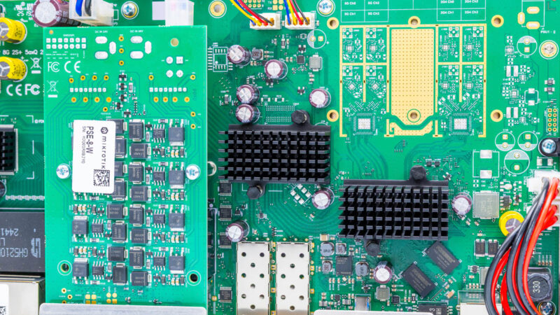
Above ports 9-16, we have the PoE+ board. This is a fairly common way to add PoE to switches that we have seen from a number of vendors (but notably not in our Cisco Catalyst C1300-8FP-2G Review.) Again, it would have been neat to have all sixteen ports be PoE+ capable or PoE++, but it would then be a different class of device since we would need large power supplies as well.
Let us get to the block diagram to see how this is all connected.


A few comments about the packet loss:
When testing with an IXIA you need to make sure that you have turned off any features that could cause the switch to generate its own traffic. This means disabling protocols like LLDP, spanning tree, router announcements, etc.
Management packets like LLDP and route announcements are typically sent with highest priority. If traffic is traversing the switch at line rate, then there’s no “idle” time on the egress port. If the switch sends an LLDP packet, then it has to drop (or queue) one of the IXIA-generated packets. This isn’t a failure, it’s the nature of a switched network.
Second, packet loss can also be caused by clock skew (also called “clock offset”). In an asynchronous network like Ethernet, one of the oscillators will always be a few “Parts per Million” (PPM) faster then the other.
The Ethernet standards allow +/- 100ppm of clock offset. This means each piece of equipment has a different view of “line rate”. One again, dropping packets due to PPM differences is not a “failure”, it’s an inherent behavior of an Asynchronous network.
Queuing can mitigate some of these effects, but too much queueing is undesirable.
I’ve made some complaints recently about various reviews, so, it’s only fair to speak up with praise where deserved.
This is “mostly” a switch. You reviewed it as a switch. And it’s also a bit of a router. You did enough of a review of that to tell us what we could expect there (NOT line rate, but not pathetic either, + everything Mikrotik). I think you hit a very good balance given your constraints.
Nice job.
Hi, is the testing being done with L3 HW Offloading enabled?
Thanks
.
“Franta February 19, 2026 At 8:52 am
Hi, is the testing being done with L3 HW Offloading enabled?
Thanks”
This is a very good question! was it conducted with Hardware Offloading enabled?