Series 3 Brings New Branding: Core Ultra X9 and X7 Join Ultra 9, 5, and 7
Speaking of SKUs, Series 3 introduces two new prefixes/tiers of chips within Intel’s traditional 5/7/9 lineup. Joining the family are the Ultra X9 and Ultra X7. The ‘X’ in this case is being used by Intel to designate chip SKUs that ship with their most powerful 12-core iGPU configuration, which will also be labeled as the Arc B390.
This is not the first time that Intel has labeled parts of their mobile chips with their most powerful iGPU (see: Iris Pro branding), but this is the first time that Intel has put that information in the name of the chip itself. The end result being that it should be easier for buyers to immediately see if a given chip SKU is using the Arc B390 iGPU.
As mentioned earlier, Intel’s launch stack for the Core Ultra Series 3 family is 14 SKUs. This will range from the Ultra 5 all the way up to the Ultra X9.
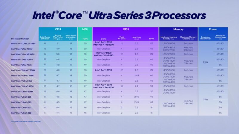
The minimum specification chip for this generation is the Ultra 5 322, which comes with 6 CPU cores – 2 P cores and 4 LPE cores – as well as 2 GPU cores. This moves up progressively through the stack until we reach the Ultra 9X 388H, a 16 CPU core tile (4P + 8E + 4 LPE) paired with a 12 core GPU tile.
All of these chip SKUs have the same 25 Watt base power rating. However, the maximum turbo power will vary between 55W, 65W, and 80W depending on the chip SKU and how the OEM has it configured. So there is significant room here for OEMs to configure chip TDPs based on their needs – something Intel needs to offer in order for Panther Lake to be able to replace both Lunar Lake and Arrow Lake.
CPU and GPU configurations aside, the various chips within the stack will also be differentiated some by their memory support. The fastest X7/X9 SKUs will support LPDDR5X-9600 memory, other SKUs will top out at LPDDR5X-8533, and some of the most basic SKUs will max out at just LPDDR5X-6800. OEMs are unlikely to want to pair more expensive faster memory with cheaper chips to begin with, but it is one more thing to keep an eye on.


While using Intel 18A is a step in right direction, Panther Lake is still wholly dependent on TSMC since the I/O tile is made by them. The 12-core GPU tile is also TSMC, while the basic one is Intel 3.
Intel is the almost only company running right way in the US’s semiconductor industry…
Losing manufacture simply means losing nation.
We can remember the fall of the UK, very easy.
Thanks for the insight Ryan, it’s been sorely missed! Not to say that Servethehome hasn’t been trying in their own way but there has been a gap since the closing of Anandtech. I am excited for this team up, keep up the great work everyone!
This might be the most exciting Intel release to me in a long time and might finally push me to upgrade my 11th Gen I series if there are some decent ultrabook models.
In my opinion having three different kinds of cores on package is not useful even from a marketing and market segmentation point of view.
The popularity of the 8-core Ryzen 9800X3D tells me people have caught on to the type of shrink-flation that increases the core count by minimising the core size.
“In my opinion having three different kinds of cores on package is not useful even from a marketing and market segmentation point of view.”
It should be largely invisible to the users. AMD has handled it well by putting lower clocking cores with identical instruction sets/IPC in Strix/Krackan Point, although the division of L3 cache is questionable.
In the future, AMD may adopt 2c/4t of Zen 6 “LP” cores in the desktop I/O die. This type of core would clearly be for improving idle power consumption, rather than increasing performance per area.
Very nicely written article!
CWF will also bring their hybrid compression bonding and, reportedly, 576MB of SRAM on the base tiles. Then NVL will, reportedly, also add SRAM on the base tiles. If they can pull off all these updates within one year, it will be long remembered.
Great Work. I’m curious why isn’t Intel; also making some of the IO dies on one of there own foundry nodes? Since the IO die doesn’t need the most advanced node and intel has experience making IO dies on both its intel 7 and intel 4/3 nodes would it not make sense to do that especially since the intel 7 fabs are not EUV fabs and thus can’t produce any of the newer nodes without major capital investments?
intel has longer term deals with TSMC and it more complicated than just we can do it, I believe that Intel has been making their IO dies with TSMC for their recent laptop chips for a while and when they have had such a crazy focus on the 18a die, going with what works probably isn’t a bad idea.
Please write about Wildcat Lake after more details become available.
“This is not the first time that Intel has labeled parts of their mobile chips with their most powerful iGPU (see: Iris Pro branding), but this is the first time that Intel has put that information in the name of the chip itself.”
Tiger Lake chips had the GPU in the name, i.e. i5-1135G7, with G7 meaning the highest GPU tier.