Intel 18A Process: Closing the Fab Gap – And Maybe Taking the Lead
As outlined earlier, outside of architecture changes within Panther Lake itself, the other big innovation for this generation of hardware is the fab node that the critical compute tile is being built on.
Intel’s 18A process node has been a long time coming for the company, and it is very close to being a make-or-break moment for the company. After falling behind TSMC by their painfully long development cycle for Intel 7, former Intel CEO Pat Gelsinger made it a priority to get Intel through 5 nodes in 4 years – essentially speed-rushing through the 4nm/3nm era in order to get Intel to the next generation of fab nodes. 18A, in turn, is the culmination of this process, intending to deliver on a cutting-edge, high-performance node that will make Intel’s fabs (and internally fabbed chips) competitive with TSMC again.
Just where Intel will land in terms of competitiveness remains to be seen (for the public, at least), but regardless of where the specific PPA metrics turn out, Intel has seemingly successfully made their big leap in fab technology: not only is Intel producing commercial wafers on 18A over at Fab 52, but they claim to be exceeding their 18A goals.
And while 18A is not make-or-break for Panther Lake due to Intel’s flexible foundry model, the reality is that everyone inside the company is a lot happier to be producing Panther Lake compute tiles on the new process node. Not only does it provide a major customer for those expensive fabs, but it means intel’s chip design teams can take full advantage of 18A’s unique abilities.
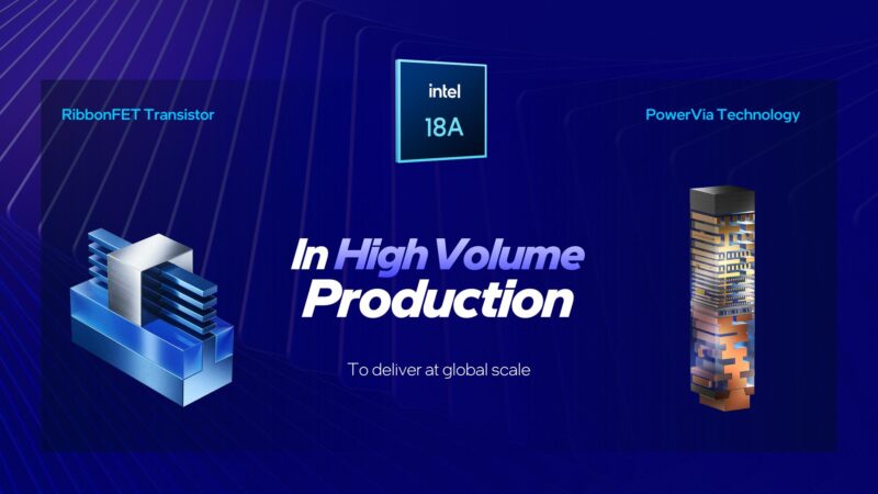
Besides the regular improvement to transistor size and power consumption from a finer node, 18A introduces two major features to Intel’s fab stack: PowerVia (Backside Power Delivery) and RibbonFet (GAAFET). This makes 18A the most important node for Intel since their 22nm process, where they introduced FinFETs and were able to reap a significant leap in transistor performance. And with 18A, they want to do much the same.
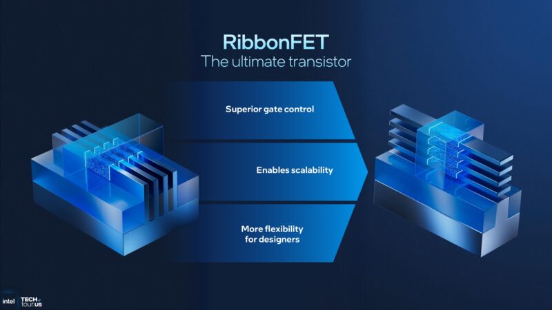
RIbbonFETs, Intel’s name for their implementation of Gate All Around FETs, is the next generation of transistor technology after FinFET. In a nutshell, it extends what FinFETs standard, and builds a gate that surrounds the transistor, rather than just fins on FinFET. The full impact of the technology is to further improve control of the gate and reduce leakage – an especially daunting task at this scale – and thereby giving transistors an extra kick in performance and energy efficiency.
Intel is not the first company to ship GAAFET products; that honor goes to Samsung. However with Samsung’s GAAFET process nodes thought to be continuing to struggle with yields, there is a chance that Intel could overtake Samsung in terms of GAAFET yields and shipments.
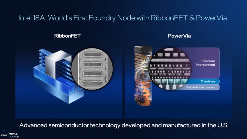
Getting back to 18A, the other major innovation here, PowerVias, is an industry-first. Intel’s name for implementing a Backside Power Delivery Network (BSPDN), the basic idea with BSPDN is to deliver power from the back side of a chip rather than the front side of it. With the front side of a chip covered in numerous metal layers above the transistors, routing both signals and power through the same space is complex and creates inefficiencies. By routing power through the relatively sparsely equipped rear, it can simplify power delivery as well as moving said power away from signal lines.
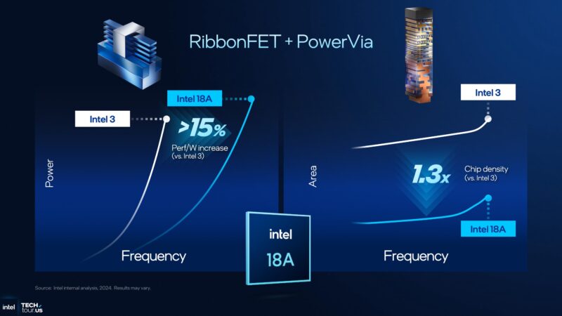
Compared to the Intel 3 process, Intel says that 18A delivers roughly a 15% increase in performance per watt at iso-power, and up to 30% higher chip density at iso-frequency. The perf-per-watt increase in particular is incredibly important for Intel, as these are the kind of fab-derived gains that regular node shrinks are no longer providing.
Ultimately, it is the combination of 18A’s transistor performance improvements and Panther Lake’s architectural improvements that Intel is counting on to deliver the one-two punch in making the Core Ultra Series 3 a competitive (and superior) SoC for the mobile market.


While using Intel 18A is a step in right direction, Panther Lake is still wholly dependent on TSMC since the I/O tile is made by them. The 12-core GPU tile is also TSMC, while the basic one is Intel 3.
Intel is the almost only company running right way in the US’s semiconductor industry…
Losing manufacture simply means losing nation.
We can remember the fall of the UK, very easy.
Thanks for the insight Ryan, it’s been sorely missed! Not to say that Servethehome hasn’t been trying in their own way but there has been a gap since the closing of Anandtech. I am excited for this team up, keep up the great work everyone!
This might be the most exciting Intel release to me in a long time and might finally push me to upgrade my 11th Gen I series if there are some decent ultrabook models.
In my opinion having three different kinds of cores on package is not useful even from a marketing and market segmentation point of view.
The popularity of the 8-core Ryzen 9800X3D tells me people have caught on to the type of shrink-flation that increases the core count by minimising the core size.
“In my opinion having three different kinds of cores on package is not useful even from a marketing and market segmentation point of view.”
It should be largely invisible to the users. AMD has handled it well by putting lower clocking cores with identical instruction sets/IPC in Strix/Krackan Point, although the division of L3 cache is questionable.
In the future, AMD may adopt 2c/4t of Zen 6 “LP” cores in the desktop I/O die. This type of core would clearly be for improving idle power consumption, rather than increasing performance per area.
Very nicely written article!
CWF will also bring their hybrid compression bonding and, reportedly, 576MB of SRAM on the base tiles. Then NVL will, reportedly, also add SRAM on the base tiles. If they can pull off all these updates within one year, it will be long remembered.
Great Work. I’m curious why isn’t Intel; also making some of the IO dies on one of there own foundry nodes? Since the IO die doesn’t need the most advanced node and intel has experience making IO dies on both its intel 7 and intel 4/3 nodes would it not make sense to do that especially since the intel 7 fabs are not EUV fabs and thus can’t produce any of the newer nodes without major capital investments?
intel has longer term deals with TSMC and it more complicated than just we can do it, I believe that Intel has been making their IO dies with TSMC for their recent laptop chips for a while and when they have had such a crazy focus on the 18a die, going with what works probably isn’t a bad idea.
Please write about Wildcat Lake after more details become available.
“This is not the first time that Intel has labeled parts of their mobile chips with their most powerful iGPU (see: Iris Pro branding), but this is the first time that Intel has put that information in the name of the chip itself.”
Tiger Lake chips had the GPU in the name, i.e. i5-1135G7, with G7 meaning the highest GPU tier.