Panther Lake Architecture: Cougars, Battlemages, and Darkmonts
Within Panther Lake’s various tiles are several new architectures across many of Intel’s functional blocks.
P-Core: Cougar Cove
Head of the class is Cougar Cove, Intel’s new P(erformance) core architecture. Cougar Cove is a further evolution of Lion Cove used in the Series 2 lineup, with Intel making specific refinements to the architecture for better performance such as widening certain queues and improved scheduling to reduce stalls in the backend execution units.
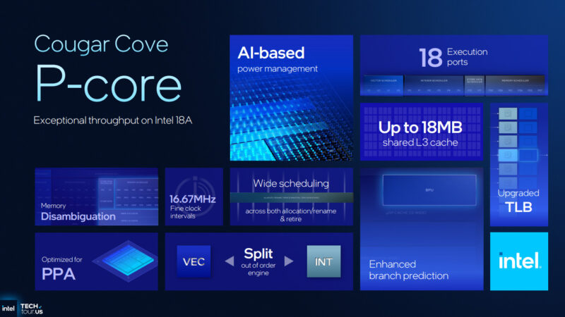
The net result is that Cougar Cove should deliver 5-10% better IPC. Is it not a significant leap in IPC – and Intel has been pretty candid on this front – but at the end of the day Intel is banking on 18A to back them up here by allowing for these mobile chips to be able to sustain higher frequencies overall.
E-Core: Darkmont
The next core type in line is Intel’s E(fficiency) core architecture, Darkmont. This is a further evolution of Intel’s previous Skymont E core architecture, though the improvements are more substantial than what went in to Cougar Cove. Darkmont is a bigger core overall, reflecting its use of a deeper out-of-order execution window and a wider frontend execution pipeline.
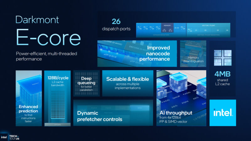
Just how much faster Darkmont will be over Skymont on a clock-for-clock basis remains to be seen; Intel has not disclosed any IPC figures, as the focus of the E cores is on efficient multi-threaded performance.
Darkmont is also the architecture that goes into Intel’s Low Power (LP)E cores. Which coming from Arrow Lake in particular represents an even bigger step up, as Arrow Lake used the even older Crestmont architecture for its LPE cores.
This change goes hand-in-hand with the larger rearchitecting of Intel’s tile design to a singular compute tile; no longer are the LPE cores sitting alone on the SoC tile, but now they sit on the same tile as the rest of the CPU cores. And while this removes part of the impetus for having low-power E cores – namely, being able to power down the CPU tile – LPE cores remain a critical part of Intel’s architecture as they are still the most efficient place to run lightly threaded workloads.
In fact, it is interesting to note that compared to Arrow Lake, Panther Lake puts a greater emphasis on the E cores than the P cores. Arrow’s 6/8/2 configuration has been replaced by 4/8/4, losing two P cores and gaining 2 LPE cores. So Intel is betting very heavily on the E cores and their LPE siblings to efficiently drive a lot of performance of the chip.
GPU: Xe3
Moving on, GPU duties are provided by Intel’s Xe3 graphics architecture. Intel has been coyly avoiding calling this their previously announced “Celestial” GPU architecture, hinting that it is more of a half-step towards it. Regardless, Xe3 marks a notable upgrade over the Xe2 architecture iGPU of Lunar Lake, and an even bigger upgrade over the dated Xe-LPG architecture used in Arrow Lake.
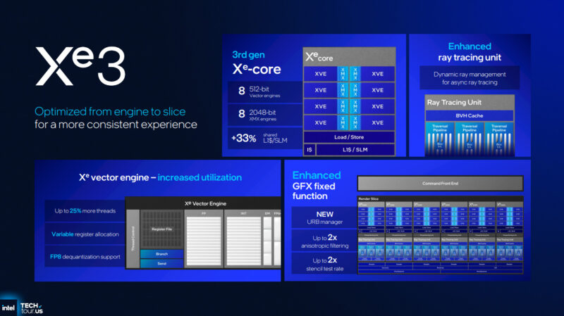
Compared to the Xe2 architecture, Intel has not made any wild changes to the core shader architecture, but they have worked to boost the efficiency/utilization of it. As well, several fixed function blocks have been improved, including a faster ray tracing unit, and doubling the throughput on certain aspects of the rasterization hardware.
But more than anything else, they have thrown a lot of hardware at the GPU. The larger, 12 Xe core tile is already 50% more Xe cores than the biggest Arrow Lake and Lunar Lake configurations – and this is coupled with a 16MB L2 cache, which is rather huge by iGPU standards. Intel is claiming upwards of a 77% performance improvement in gaming workloads at iso-power, a significant improvement to say the least.
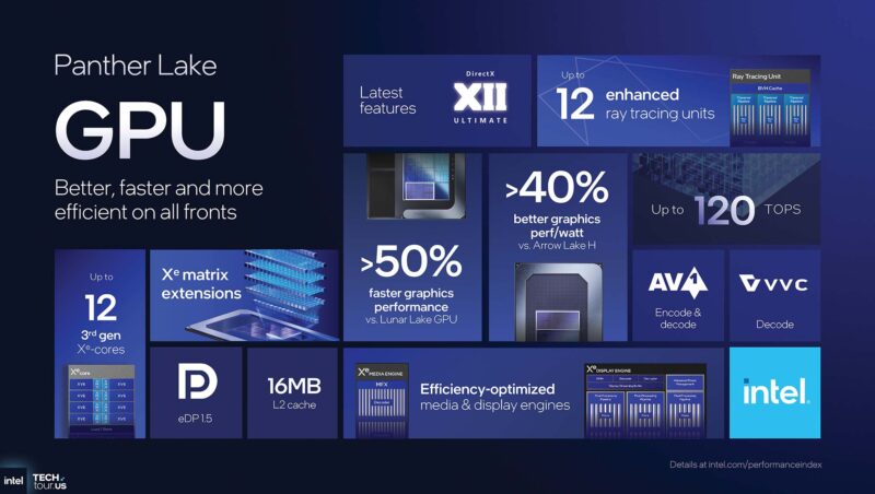
Otherwise, one of the major selling points for Intel’s iGPU is simply the that it is a modern GPU design. With ray tracing hardware, XMX matrix units, and full DirectX12 Ultimate compliance, the Xe3 architecture iGPUs are capable of running all of Intel’s latest image enhancement technologies. This includes both the latest iteration of their XeSS image upscaling tech, as well as their frame generation/interpolation technology. Competitively, this helps them keep parity with NVIDIA’s discrete GPUs, and it is a major feature differentiator from AMD’s Strix Point/Halo hardware, which uses a GPU architecture that lacks matrix cores – and thus making them unable to use AMD’s latest image enhancement technologies.
NPU: NPU5
Pulling dedicated AI duties for Panther Lake is Intel’s integrated NPU, which is now in its fifth generation and aptly named NPU5. Following an arms race in NPU performance in the past couple of generations in the PC space, Intel’s NPU5 architecture features more modest aims. Rather than improving top-line performance, Intel has opted to optimize the size of the NPU block itself, claiming that their latest design offers 40% more TOPS per mm2 of die space. Which, with performance holding steady at 50 TOPS of INT8, means that Intel has saved significantly on expensive 18A die size in NPU5.
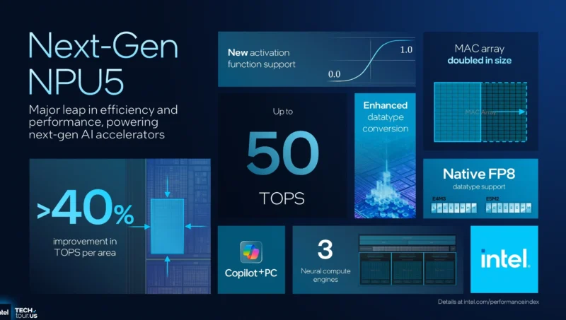
And while INT8 performance has not increased generation-over-generation, Intel has added FP8 support to the NPU as well. Which means for models that are suitable for inference at low floating point precisions, those models will be significantly faster versus having to run in FP16 on earlier NPU designs. In practice this a bit of Intel keeping up with the rest of the industry, as well, where cutting-edge models can run as low as FP4.
I/O: Wi-Fi 7 R2 & Thunderbolt 4
Finally, Intel’s I/O connectivity is somewhere between a side-grade and a minor upgrade with the Panther Lake platform. While Intel is promoting Thunderbolt 5 support for this generation of devices, the platform itself does not natively support Thunderbolt 5. Rather, the platform (still) only features native support for Thunderbolt 4. For laptops that do feature Thunderbolt 5 connectivity, this is being provided via an external controller.
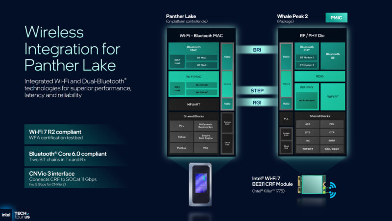
Wi-Fi, on the other hand, does bring some new hardware with the accompanying BE211 module. As with its predecessor, BE201, this is a CNVio3-connected module that holds the PHY and RF components for Wi-Fi and Bluetooth, while the MAC is integrated into Intel’s platform controller. In conjunction with Panther Lake, BE211 brings support for additional features laid out with the impending release of Wi-Fi 7 Release 2, including multi-link reconfiguration and P2P channel coordination.
The combined platform also brings support for Bluetooth 6.0, the first Intel platform to support this iteration of Bluetooth. The most notable addition here is channel sounding support, which allows Bluetooth to pinpoint the location of a BT client to within 10 centimeters or so for improved “find my” device location accuracy. Intel is also implementing a second BT radio here, with the idea being to use both radios to improve the distance of Bluetooth communications (similar to how multiple streams works for Wi-Fi).


While using Intel 18A is a step in right direction, Panther Lake is still wholly dependent on TSMC since the I/O tile is made by them. The 12-core GPU tile is also TSMC, while the basic one is Intel 3.
Intel is the almost only company running right way in the US’s semiconductor industry…
Losing manufacture simply means losing nation.
We can remember the fall of the UK, very easy.
Thanks for the insight Ryan, it’s been sorely missed! Not to say that Servethehome hasn’t been trying in their own way but there has been a gap since the closing of Anandtech. I am excited for this team up, keep up the great work everyone!
This might be the most exciting Intel release to me in a long time and might finally push me to upgrade my 11th Gen I series if there are some decent ultrabook models.
In my opinion having three different kinds of cores on package is not useful even from a marketing and market segmentation point of view.
The popularity of the 8-core Ryzen 9800X3D tells me people have caught on to the type of shrink-flation that increases the core count by minimising the core size.
“In my opinion having three different kinds of cores on package is not useful even from a marketing and market segmentation point of view.”
It should be largely invisible to the users. AMD has handled it well by putting lower clocking cores with identical instruction sets/IPC in Strix/Krackan Point, although the division of L3 cache is questionable.
In the future, AMD may adopt 2c/4t of Zen 6 “LP” cores in the desktop I/O die. This type of core would clearly be for improving idle power consumption, rather than increasing performance per area.
Very nicely written article!
CWF will also bring their hybrid compression bonding and, reportedly, 576MB of SRAM on the base tiles. Then NVL will, reportedly, also add SRAM on the base tiles. If they can pull off all these updates within one year, it will be long remembered.
Great Work. I’m curious why isn’t Intel; also making some of the IO dies on one of there own foundry nodes? Since the IO die doesn’t need the most advanced node and intel has experience making IO dies on both its intel 7 and intel 4/3 nodes would it not make sense to do that especially since the intel 7 fabs are not EUV fabs and thus can’t produce any of the newer nodes without major capital investments?
intel has longer term deals with TSMC and it more complicated than just we can do it, I believe that Intel has been making their IO dies with TSMC for their recent laptop chips for a while and when they have had such a crazy focus on the 18a die, going with what works probably isn’t a bad idea.
Please write about Wildcat Lake after more details become available.
“This is not the first time that Intel has labeled parts of their mobile chips with their most powerful iGPU (see: Iris Pro branding), but this is the first time that Intel has put that information in the name of the chip itself.”
Tiger Lake chips had the GPU in the name, i.e. i5-1135G7, with G7 meaning the highest GPU tier.