
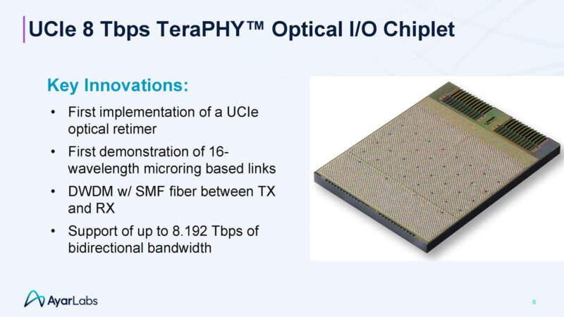
Ayar Labs has a UCIe optical I/O retimer that it is showing off at Hot Chips 2025. The basic idea is to make a UCIe chiplet that makes it easy to integrate optical I/O into a package, since it is standards-based. The chiplet also provides a lot of off-package bandwidth since it is an 8Tbps class device.
Please excuse typos since we are doing these live.
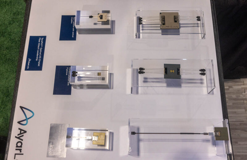
Ayar Labs UCIe IO Optical Retimer at Hot Chips 2025
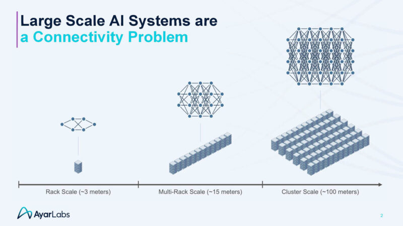
One of the biggest challenges today is scaling up from thinking of thousands of chips connected as a big cluster to thinking in terms of millions. That makes the interconnects a big deal. Primarily, this is happening in AI.
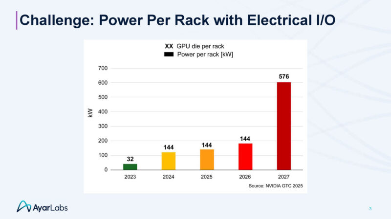
A big challenge is the power density per rack.
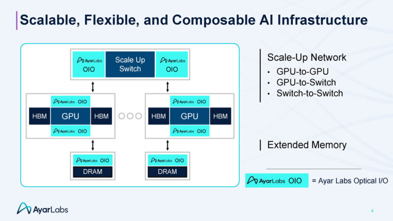
Ayar Labs has an optical I/O chiplet to help scale-out using optics.
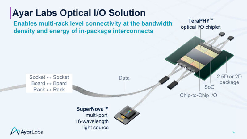
Here is the Ayar Labs TeraPHY optical I/O chiplet and the SuperNova light source.
We covered the Ayar Labs TeraPHY at SC23.
The company has a UCIe optical I/O chiplet. UCIe is a standards-based way for companies to build packages to common specs to make them easy to integrate.
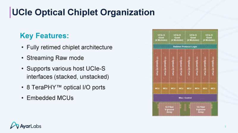
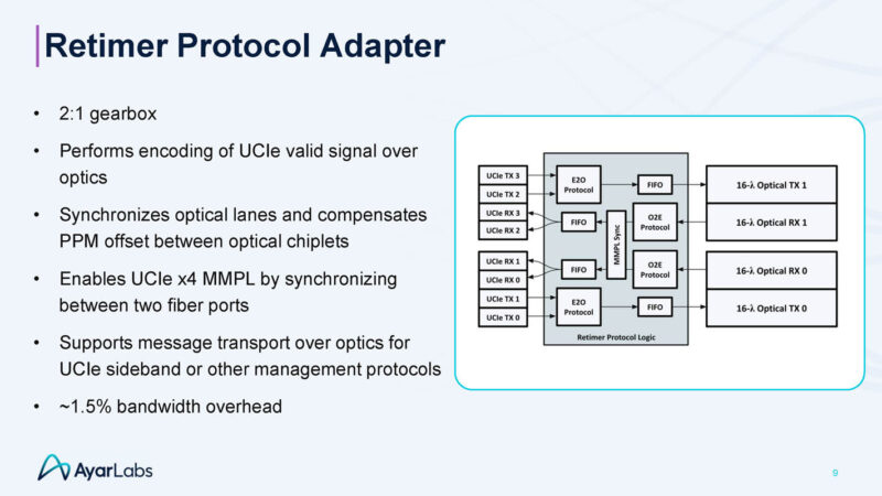
Here is how the UCIe chiplet is organized.
Here is the architecture:
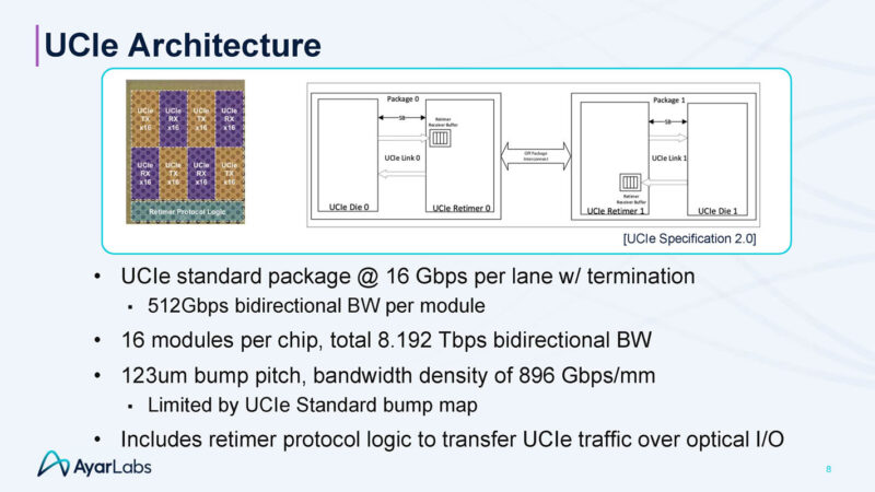
There are UCIe receivers, then the data is retimed, then it goes to the optical side. That helps decouple the optical and electrical signaling challenges.
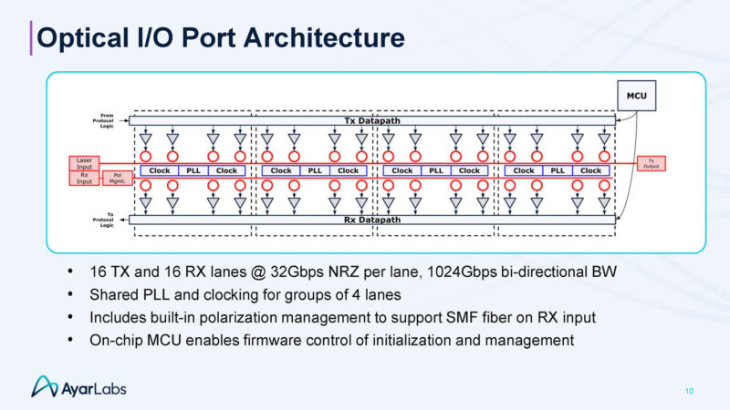
Here is the port architecture.
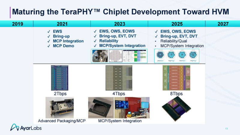
We have seen Ayar Labs for years. Now they are at 8Tbps on the chiplet and it seems more refined.
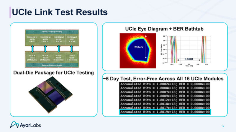
Here are the UCIe link test results
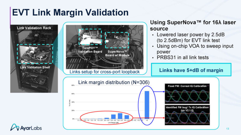
Here is the link margin validation:
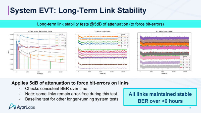
The company is also testing the long-term link stability.
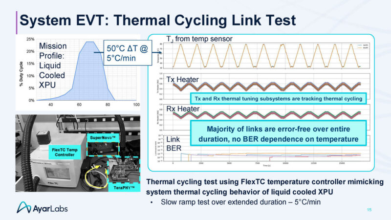
Here is the thermal cycling. This is a big deal because as chips heat and cool, that can cause materials to expand and contract and that can actually change how light flows through channels.
Here is a co-packaged 500W device. That is more of a modern CPU TDP instead of an AI accelerator TDP that is often 2-3x that today.
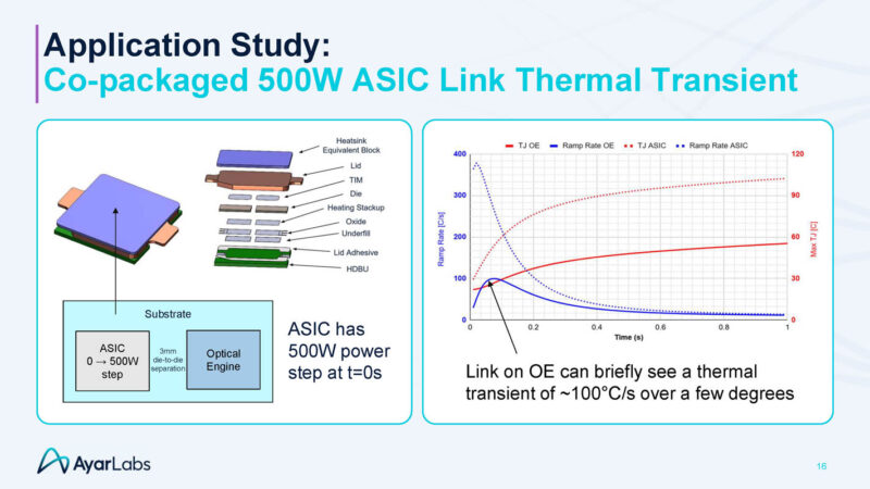
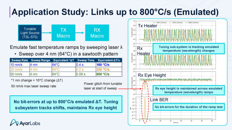
This is an emulated thermal ramp test:
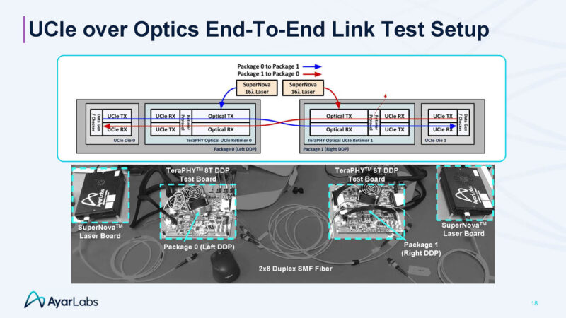
Here is an end-to-end link setup. Ayar Labs said while they are showing the EVT here, they are now well into DVT towards getting to high-volume manufacturing.
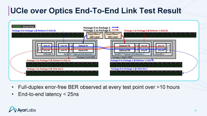
Here is the 10 hour link test result doing end-to-end testing.
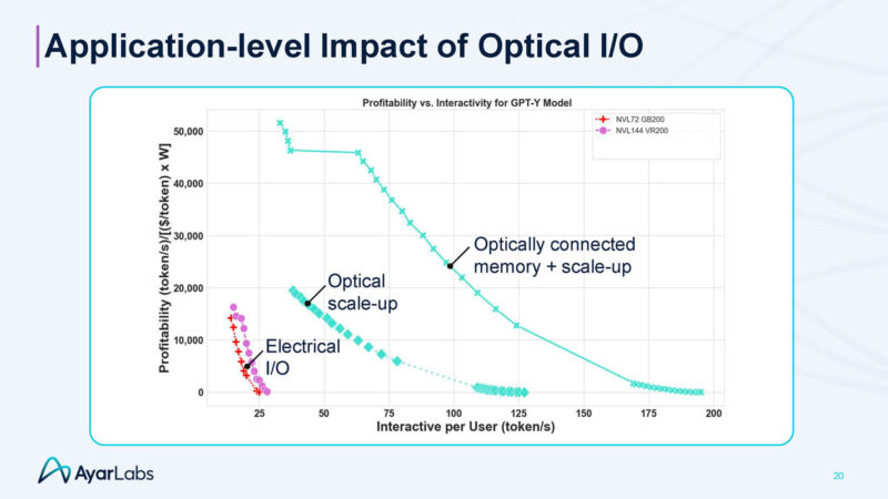
The idea is that using optical I/O, the interconnects can grow and therefore systems can grow larger than is possible with electrical I/O.
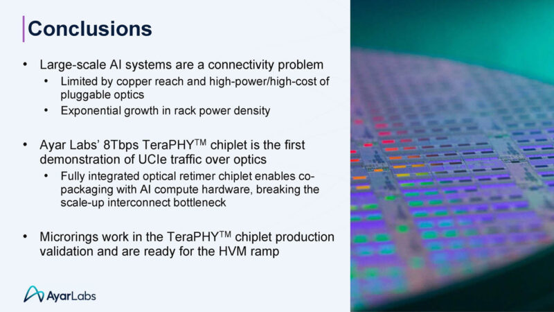
Here is the wall of text conclusions slide.
Final Words
With UCIe, this is interesting. At the same time, if this is not in high-volume manufacturing today, it is not something we would expect to see in chips we buy in the next year. Still, there is a big push in the industry for electrical I/O and one very valid approach is to just standardize the chiplet using UCIe and make it “easy” for folks to integrate into packages.


