
Alongside AMD’s numerous client-focused hardware announcements during their CES 2026 keynote, the company also devoted a bit of attention to their data center/server products. Though the company is essentially mid-cycle on its major data center products right now – and thus is not launching anything in the immediate timeframe – AMD still opted to use the attention garnered by hosting the official opening keynote for CES to outline the status of its 2026 server products.
EPYC “Venice”
Notably, both AMD’s next-generation server CPU and next-generation server GPU were on display in some fashion. First off is Venice, the codename for AMD’s next-generation EPYC processor based on the Zen 6 CPU architecture. While AMD Venice has been a staple of AMD’s data center CPU roadmap for some time now, and the company has previously gone into high-level details about the chip, CES 2026 marked the first occasion where they’ve shown off the actual silicon.
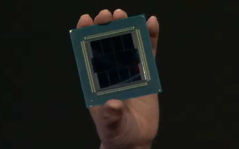
This week’s show and tell did not come with any new information on the specifications for the chip itself. But for the first time we can see how the chip is laid out, something that garnered increased interest after AMD revealed last fall that Venice would rely on 2.5D packaging.
When it launches later this year, Venice will bring several firsts for AMD’s EPYC lineup. Enabled by the aforementioned 2.5D packaging, the heart of the chip is now comprised of what appears to be two I/O Dies (IODs) at the center of the chip. Then directly flanking those IODs are 8 CCDs holding the Zen 6 CPU cores. This is fewer CCDs than found on the current Zen 5 Turin processor (which houses 16 of the things), but it is more CPU cores altogether, as AMD has previously indicated that Venice will have 256 CPU cores. AMD has previously disclosed that the Zen 6 CCDs used in Venice will be built on TSMC’s forthcoming 2nm process.
Otherwise, the biggest question mark with regards to physical hardware is the 2.5D packaging used – if AMD is throwing everything on a large silicon interposer here, or using a finer fan-out solution (ala Navi 31). All of which we expect will be disclosed a bit later in the year as AMD gets closer to shipping the silicon.
Instinct MI455X (& MI500, too)
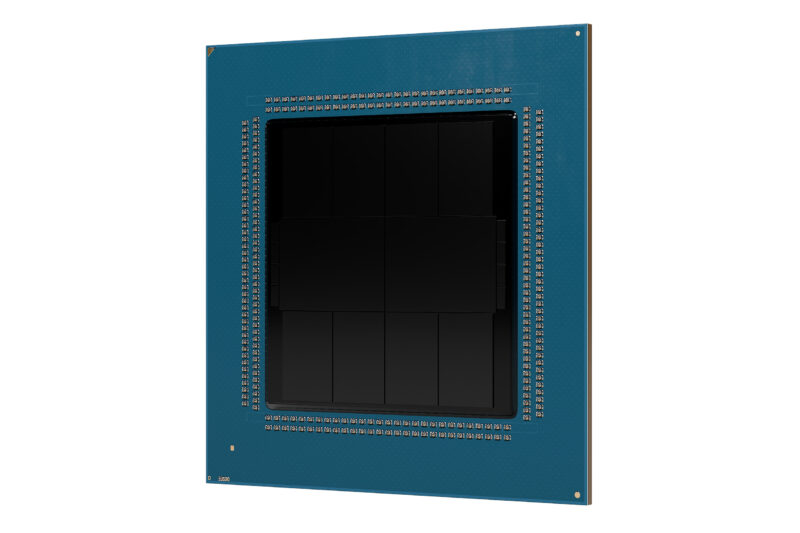
Alongside our first look at Venice, AMD CEO Dr. Lisa Su also had its GPU counterpart, MI455X, on-hand and in-hand.
As with Venice, this marks the first time that AMD has shown off the next-generation server GPU. And, fittingly, it is an even bigger deal for the company, both in terms of its sheer size – between its chiplets it is comprised of 320 billion transistors – and in terms of AMD’s plans for expanding their share of the server market.
Unlike Venice, AMD has not sent along any full chip renders. But the chonky chip is big enough to easily see even from the broadcast cameras focused on stage. Multiple chiplets are surrounded by 12 36GB HBM4 memory stacks. AMD tells us that there are 12 chiplets overall – with some covered by the 3D die stacking – which are being fabbed on a mix of TSMC 2nm and 3nm process nodes.
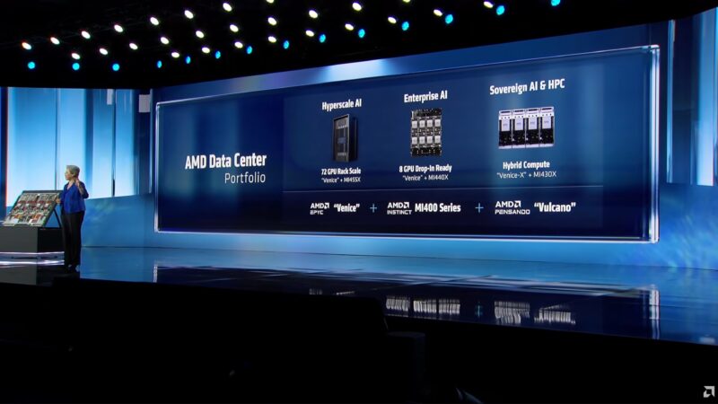
Previously, AMD had disclosed two MI400 series SKUs: the flagship MI455X for AI, as well as the more nebulous MI430X, a chip with faster FP64 for HPC use cases. These two chips, as it turns out, will be joined by the MI440X, which appears to be a scaled-back version of the MI455X. Specifically, AMD is pitching it at 8-way GPU servers, which is in contrast to MI455X’s rack-scale ambitions. There are no further technical details on the chip, but presumably AMD is pruning its power consumption – and possible some I/O – in order to get something that works better in a traditional server node.
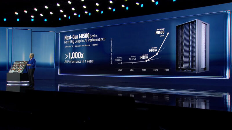
Su also used the presentation to reiterate that AMD’s current public roadmap goes out to the MI400 series’ successor, the MI500 series. The company has previously disclosed that the MI500 series will be released in 2027 – in keeping with their annual data center GPU release cadence – and for CES they have delivered some high-level details for the first time. As expected, the chip will be based on a newer CNDA architecture, CDNA 6, and will be fabbed on an “advanced 2nm” process, and will be paired with HBM4e memory. As with the launch of the MI400 series, expect an on-time launch for the MI500 series to be in the latter part of 2027.
Helios, AMD’s First Rack-Scale System
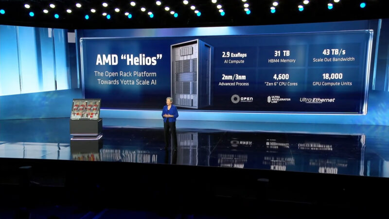
Ultimately, both Venice and MI455X are meant to be a bigger part of a whole – that whole being AMD’s Helios rack, which was the final data center reveal of the night. When it launches later this year, Helios will be AMD’s first scale-up rack scale system for data center AI processing. As a result, it is a very big deal for AMD, as it is both a vehicle to sell lots of AMD chips stuffed throughout the rack, but also to give them an in-house product to rival NVIDIA’s NVL72 racks.
AMD disclosed Helios back at their 2025 summer data center event, but like the rest of the data center hardware discussed during CES, the show marked the first time it was revealed to the public.
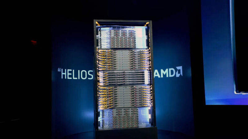
Helios is, in short, a beast. AMD has opted for a double-wide rack for Helios, making it twice the size of a typical server rack. And at nearly 7000 pounds it is quite heavy as well.
As AMD was showing off a full Helios rack, they also had a single compute tray propped up to show off what it is made of.
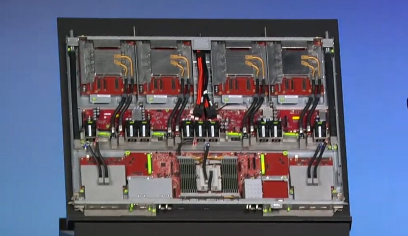
Helios will include 18 compute trays, each housing 4 MI455X accelerators and a single Venice CPU, giving the complete system a total of 72 GPUs and 18 CPUs – or breaking that down into core counts, about 18,000 compute units and 4,608 CPU cores. All told, the monster rack is slated to offer 2.9 EFLOPS of FP4 compute performance for AI workloads. As well, all of the racks are equipped with networking gear from AMD’s Pensando division, providing the critical scale-out capabilities that make Helios such an important product for AMD.
As with the rest of AMD’s data center product stack, Helios is slated to be released later this year.


AMD’s packaging for Venice is a huge leap forward. Removing the SerDes links between chiplets will increase bandwidth and reduce latencies which should improve multithreaded performance across the chip greatly. I do wonder if the two IO dies used are identical and just rotated 180 degrees with respect to each other. That would keep the design simple and promote economies of scale. What is interesting is that the 256 core figure is likely with the Zen 6c cores for density and not the higher clocked, V-cache capable units which should be 12 core chiplets. That puts an effective limit at 96 cores for those gunning for higher clocks and/or V-cache.
Personally I am surprised at how square the Venice packaging is. I would have thought AMD would leave some room to grow to additional chiplets for things like GPU compute, FPGA, or on-package networking without the need to remove CPU chiplets. I see this as being particularly noteworthy as networking is quickly moving to copackaged optics on the switch side and it is only a matter of time before server chips like this include 800 Gbit/1.6 Tbit networking inside of the socket. The big benefit here is that PCIe lanes off of the IO die will not need to be leveraged for network interfaces while simultaneously providing lower network latency.
Also worth calling out the 16 DIMM slots for Venice in the compute trays. As widely rumored before, it appears that Venice will support 16 channel memory. Without some major changes to memory (see CAMM), this is the effective limit for how many memory channels can hang directly off of a socket. This highlights what DIMMs are for nowadays: pure memory capacity. HBM has taken over for latency, bandwidth and density.
MI455X is an impressive chip in terms of packaging as well but also feels a bit iterative given that AMD did something similar last generation. I do wonder if we’ll see custom implementations of this design mixing and matching a number of Zen 6 chiplets. Last generation AMD produced a custom part for Microsoft’s Azure cloud that only had Zen 4 CPU chiplets. Four sockets of 256 cores of Zen 6c with 432 GB of HBM4 memory each would be impressive for CPU based workloads.
AMD’s strategy feels like they’re rapidly moving toward a schema where CPU and GPU compute are interchangeable. I wonder how long it’ll be before AMD attempts a checkerboard pattern of CPU, GPU and HBM on a wafer scale interposer (think Cerebras large but chiplets). Just use a full wafer as the interposer that all the chiplets are mounted to. Put dedicated IO dies around the edge for things like networking and PCIe. It seems that the packaging tech is there to do it. Don’t ask how much power and cooling such a setup would be.
Imagining co packaged optics on a server cpu…sounds great, but also what sort of socket installation procedure is that going to be. Not that many of us still replace CPU’s on servers…but aren’t most of those switches with CPO are a BGP switch-chip. Neat to think about.
Anyway, agreed on that package size, should have room for expanding the CPU tiles. Extending the x86 capability is the way to stave off RISC/ARM or whatever comes next. This is the way. In the way of that though might be the socket compatibility or some other limitation that keeps it from getting bigger.
Do you have any idea what those four mini chiplets to each side of the IODs are?
AMD has not officially said. I suspect they’re either blanks (structural silicon) or some kind of electronics, but no way to know for sure right now.
Could it be possible that those are PCIe-PHYs? My idea is that maybe AMD connects the IODs to each other directly using Fan-Out, and to go off-package can add the PHYs to the same interface. Would allow to use the same IOD twice instead of a mirrored design and also to have smaller variants (1 IOD+4 CCD) with the same amount of PCIe Lanes.
@MDF While not copackaged optics, Intel did have on package Omnipath interfaces during the Sky Lake/Cascade Lake generation. So there was some cabling running to the ‘wings’ of that socket for the interface. Systems that supported on-package Omnipath had a slightly different bracket on the motherboard to account for the different CPU socket shape. Any sort of copoackaged optics would need to do the same. This does increase system setup time due to the additional steps to connect the optical cables and ensure that they’re routed properly in the chassis.
I don’t think that AMD is close to the maximum socket size for what can be assembled. I know off hand that there are even larger packages, though most of those are ceramic server chips from IBM. What might be the more limiting factor is not the socket size itself but motherboard limitations for housing that socket. Server motherboards are becoming rather cramped with lots of DIMM slots. Given a certain number of memory channels, there likely is a maximum socket size system designers would tolerate. With what AMD does have, there is still a little bit of room to leverage two larger chiplets in the corner of the current arrangement. Conceptually a FPGA or a small GPU chiplet could fit into these posts for a different style of compute in the server socket. Perhaps AMD will factor in more grow when they jump to DDR6 in a few years , SOCAMM and/or go full CXL memory expansion.
In terms of topology, AMD is still leveraging the IO dies as the means to handle routing coherent traffic between the chiplets. This seems to be an aggregation step which also includes the memory controller. Venice does change things up by leveraging two IO dies this time around. I would expect in the future AMD would include a coherency router on the main chiplet and go with a simple cardinal mesh link between chiplets directly (north, south, east, west) while moving the IO dies to the edge of the socket. This simple grid style design would only be limited in scale by room in the socket, power and cooling. This is similar but not exactly how Intel is leveraging chiplets in server. For Intel, they place a memory controller on each CPU chiplet which may or may not be leveraged based on socket IO (ie Intel can put in more chiplets than there are external memory channels). I do think it is wiser to keep the memory controller and PCIe as its own chiplet that sits on the same on package fabric between chiplets. Depending on the socket needs (SP5 vs. SP6 vs. AM5), only the number of IO dies needed would change to scale up.
@Stefan The IODs are flip-chips with I/Os all across their surface, not just at the edges. Genoa supported 128 + 8 = 136 PCIe lanes (differential pairs) from a single processor socket. If Turin has the same number of PCIe lanes, that would be 136 signals on each side of the processor package going in and out of 4 mini chiplets. Chips and Cheese suggested the mini chiplets could be decoupling capacitor chips to keep the voltage stable for high-speed single-ended DRAM signals.
It’s interesting that AMD reduced the number of CPU chiplets from 16 to 8 and went with larger size CPU chiplets. That suggests confidence in TSMC’s N2P yield or confidence that their design can isolate a defect so that a defect won’t ruin a whole chiplet. I agree with Kevin G that the 256 core Venice processor must be using low clock frequency Zen6c dense cores even if AMD calls them “Zen6” cores. The Venice processor with real Zen6 (high clock frequency) cores will probably contain about 192 cores to have an achievable improvement in performance/Watt from Zen5. A 192 core Venice processor could be organized as 8 chiplets with 2 CCX per chiplet and 12 cores per CCX. Desktop processors will probably have a single CCX with 12 Zen6 (high clock frequency) cores.
At CES, AMD also mentioned Venice-X, which has 3D V-Cache like Milan-X and Genoa-X. The 96 core version of Genoa-X has 12MB of L3 per core. Some media outlets have reported that Venice-X will have the option for a stack of two 3D V-Cache die under each CPU chiplet. Two 3D V-Cache die would provide 4 + 8 + 8 = 20MB of L3 per core. A 192 core Venice-X Zen6 processor could have:
192 x 12MB = 2304MB = 2.25GB of total L3 (one 3D V-Cache die per CPU chiplet) or
192 x 20MB = 3840MB = 3.75GB of total L3 (two 3D V-Cache die per CPU chiplet).
For Venice-X, each high clock frequency Zen6 CCX with 12 cores per CCX would share 12 x 12MB = 144MB or 12 x 20MB = 240MB of L3 cache. For comparison, the largest Granite Rapids processor in SNC3 mode has 43 cores sharing 168MB of L3 slices, with the whole processor containing about 3x that.
The pic of her holding it… Never thought I’d say this but, a banana for reference would’ve been nice!