
At STH, we hear of a new startup with new accelerators more than once a week. NextSilicon is different for a few reasons. Its new Maverick-2 chip has customers like Sandia National Lab for its HPC part. It is also doing something NVIDIA is not: it is focusing on accelerating FP64 just as NVIDIA moves away from the space. Further, this is not a first-generation product. Instead, NextSilicon’s data flow architecture has found its way to another generation, with more planned. All this is to say that the NextSilicon Maverick-2 is far from slideware. It is set to be a commercially viable product which matters when accelerator startups saying they have something better than NVIDIA crop up faster than bean sprouts.
Why NextSilicon Went Dataflow Architecture
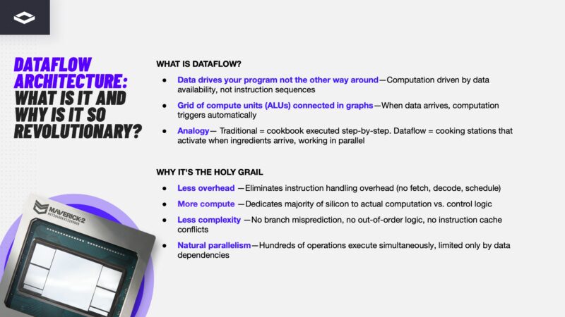
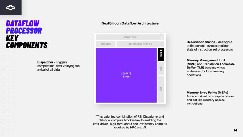
Instead of a traditional Von Neumann architecture, NextSilicon is a dataflow architecture. The idea is that instead of a typical CPU or GPU where instructions are executed sequentially based on a program counter and there is a single memory space for instructions and data, dataflow architectures execute an instruction as soon as its required data is available.
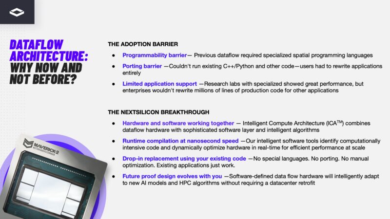
NextSilicon may be a startup, but it has 40% or so of its 400 employees working on the software side. The goal of NextSilicon’s software is to find hotspots in applications, and bring them to the dataflow engine for execution without costly porting.
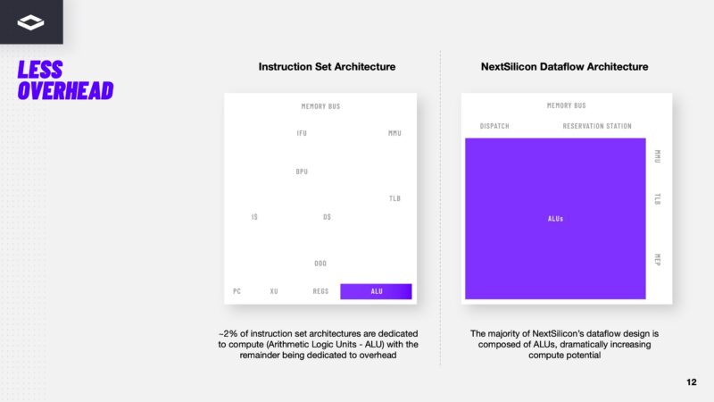
Here is the idea, the arithmetic logic units or ALUs can be a much higher proportion of a chip because instead of having decode engines, lots of memory management, and so forth, data comes into the chip and then flows through the ALUs.
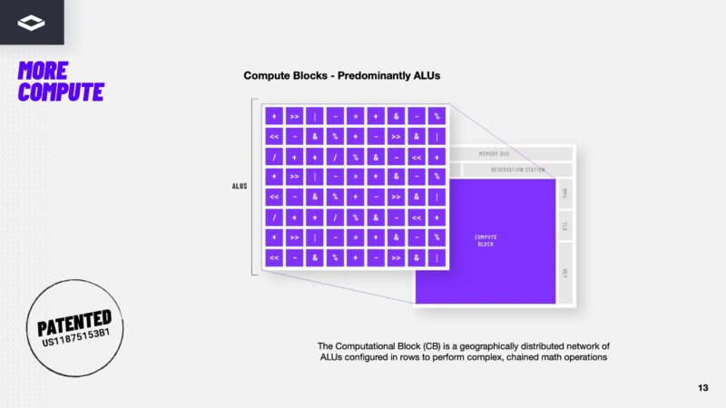
Maverick-2 has big compute blocks with ALUs to allow for data to flow through the chips and have calculations performed as the data moves.
NextSilicon has patents on how all of the units that make this work come together, but the key here is that instead of going through a program counter and instructions, the design of these chips is such that as data arrives, it immediately starts computation. This might seem trivial, but if you think about a typical CPU where a ton of compute resources go to functions like branch prediction and speculative execution because the chip is waiting for data, then it starts to make more sense on what the company is doing. The idea here is that the ALUs are fed with their configuration, or the operations they will perform, and then the chips job is to just pull as much data as possible into the chip so these math units can get data, do their thing, and then pass off the result to the next step.
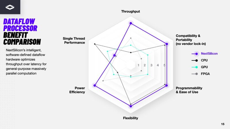
As you might imagine, NextSilicon says that its chips are better than CPUs, GPUs, and FPGAs.
Having an idea for a dataflow processor is one thing. Having silicon and cards that organizations can buy, deploy, and use is another. That is where Maverick-2 comes in.
NextSilicon Maverick-2 Brings Data Flow and HBM3e to HPC Customers
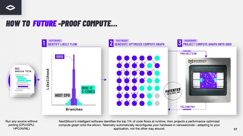
How NextSilicon is making this work is that its software looks for hot spots in code. Think of these like the matrix math operations in AI or HPC applications where a ton of compute is focused on a certain spot. Call it the 5% of code that requires 95% of the computation, 1% / 99% or whatever ratio you want to ascribe it. From there, NextSilicon generates a compute graph and places it onto the compute grid on its accelerators.
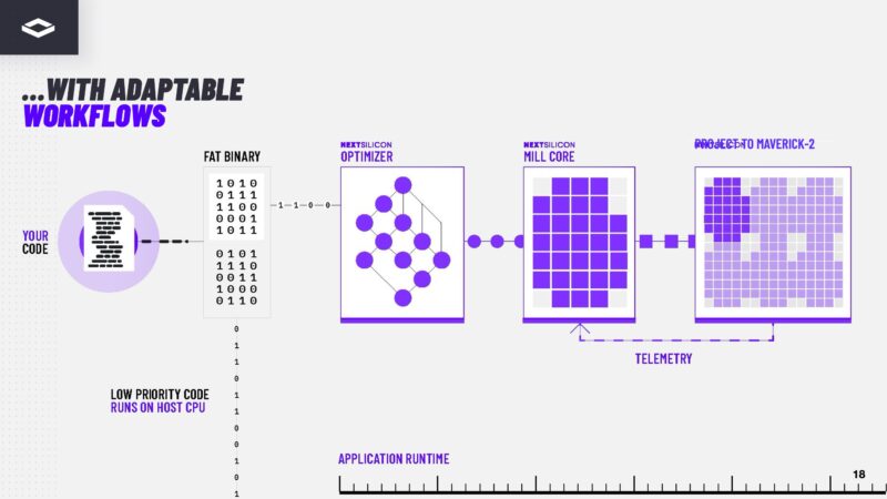
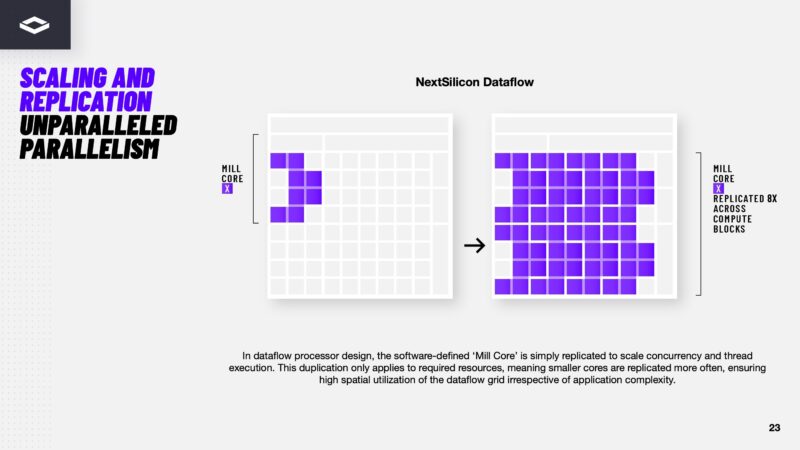
NextSilicon’s software creates Mill Cores which have the series of operations that need to be performed on the data and then places those on its compute tiles.
Here is what it looks like in another visual going from source code, to a representation of operations, then bringing that to a traditional instruction set processor.
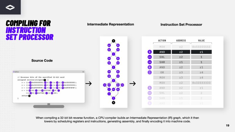
In the dataflow architecture, instead of having to go to instruction sets, the dataflow is generated to look like the representation of instructions.
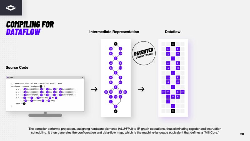
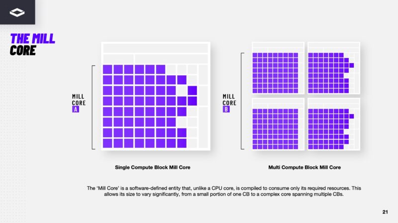
The Mill Core is compiled to only have required resources so that the software can place as many of these onto the silicon as possible to optmize throughput.
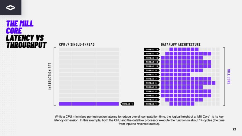
Here is another difference between a latency optimized CPU core and a Mill Core in the dataflow architecture.
Here is how NextSilicon shows it can place many Mill Cores onto its silicon to scale compute.
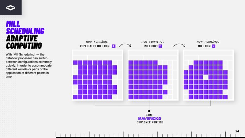
The same chip can run different Mill Core configurations by changing how the flows should happen across the chip. If you were to squint a a high-level this is somewhat analogous to how you might think of a FPGA insofar is that you have the flexibility to reconfigure compute. This is not a FPGA, but the idea of this flexibility across the silicon is similar.
Perhaps the best way to think of this is that instead of trying to map software to a CPU or GPU pipeline, NextSilicon analyzes the software, then maps its accelerator hardware to the software. Still, it needs hardware. For that, NextSilicon has Maverick-2 as well as a Arbel RISC-V processor. The Maverick-2 has RISC-V control processors but Arbel is designed to be a host CPU.


This reads like yet another “revolutionary” startup PR push for IPO cash-out.
The performance claims are simply insane, and worth nothing without independent verification. They also claim the ability to run unmodified C++, Python and *CUDA* code.
It’s highly unlikely that Arbel at 2.5GHz matches Zen 5 that clocks well over 5GHz in general performance. Maybe some specific micro-benchmark, but without knowing more about what they base their claims on it’s just noise.
Kyle, you seem very pessimistic. Custom software defined silicon is an awesome technology that will be great to watch advance. Like stated in the article these chips are beyond just “slideware” and have been in validation since 2022 with actual deployments now existing. While yes a lot of benchmark slides read like advertising slides (because a lot of time that is what they are) it is weird to read this great article and skip all of the great details over the function of these accelerators. STH is not calling on us to personally go out and fund this company they are instead disseminating information that would normally be harder to access, and understand without the helpful commentary.
@Rainey
I’m pessimistic because I’ve seen this MO time and time again. Since they supposedly have a US national laboratory evaluating the chip I’ll wait for a proper peer-reviewed paper that will vindicate their PR. Until then it’s just unsubstantiated claims.
We’ve seen the software-driven hardware performance claims before – Intel Itanium relied on magical compilers that never came for the massive theoretical performance increases. This seems to even claim that unmodified C++, Python, Fortran and CUDA can run on it. Each of those took decades to get right. CUDA compatibility is a red flag since both Intel and AMD abandoned their own compatibility efforts with ZLUDA due to legal issues.
There’s being optimistic and there’s being unrealistic. If these claims can be verified by trusted third parties then great, we have a solid contended to disrupt the market.
Dataflow can extract parallelism from algorithms without you having to code it. However, the patents are almost certainly worthless garbage because dataflow is nothing new. I worked at a startup trying to bring dataflow CPUs to the market over 20 years ago. They had full working CPUs implemented in an FPGA. I repeat: *EVERYTHING* I see in this has been done a *LONG* time ago so there will be prior art on it *ALL*.