
Microsoft today showed a new approach to cooling the world’s hottest AI accelerators and other chips. The company is etching complex microfluidics channels directly into silicon to achieve greater cooling efficiency for future generations of chips.
Microsoft Etches Complex Microfluidics Channels Directly into Silicon Chips
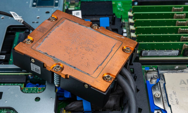
In the current model, coolant passes through a cold plate’s microchannels and then contacts a chip package with some thermal interface material between the plate and the CPU. This approach involves multiple layers, which reduces efficiency.
Each time there is a new material, that makes the thermal transfer less efficient. Microsoft is now looking at creating microfluidic channels etched into the chip itself to increase surface area and cooling performance. Microfluidics channels have a number of benefits beyond just directing flow as different forces are at play. An example is that surface tension is a much more important force in microfluidics than it is in a typical coldplate design.
Microsoft did not say which chip it used as a test vehicle. Microsoft was focused on the AI applications, but the chip looks like it is actually a 3rd Gen Intel Xeon. Here is an Ice Lake generation Intel Xeon Platinum 8362.
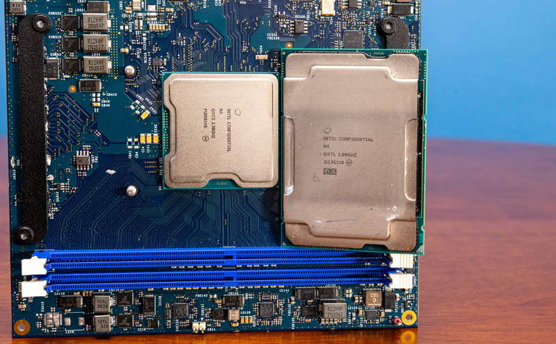
We can also see that installed in the server, we appear to have DDR4 RDIMMs and 8-channel memory which would also point to a 3rd Gen Intel Xeon Scalable part. It is also has Wiwynn memory. Of course, this could also be something very custom, but perhaps Microsoft just did this project using older chips. To give some sense, the standard 3rd Gen Intel Xeon Scalable parts only went up to around 270W TDP.

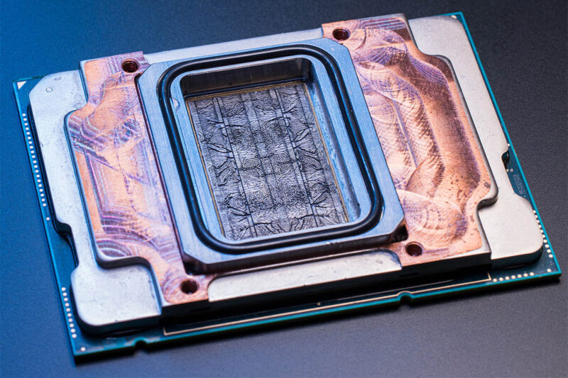
Part of the challenge with designing a solution like this is that Microsoft needed to etch the channels directly into the silicon with enough depth that surface area and flow would hit targets. At the same time, too deep and it can cut into the structural rigidity of the chip.
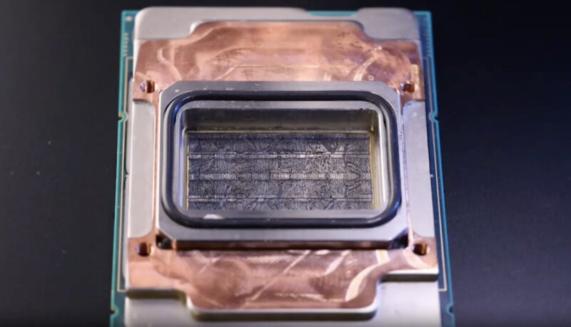
Microsoft also needed to design a leak-proof package to bring fluid to and from the chip.
Final Words
This is neat technology. We have seen other companies like Fabric8Labs ECAM Enabled Thermal Solutions where the future might be printing channels directly on the silicon itself. In the future, with 3D packaging, there will be a need to cool multiple chips in a stack. Microsoft did not announce using this in any current CPUs, but it was neat to see a test chip built around an older CPU.


Wouldn’t constant flow like in a river cause abrasion/erosion of the chip surface?
There’s more info about the tech on the Corintis website which was Microsoft’s partner for the research on this.
https://corintis.com
there shouldn’t be any abrasive solids (or any solids) in the cooling medium. in a river u have gravel and stuff which are the cause for a river to carv its way thru solid rock.
would be interesting to see how they came up with the pattern of the channels. also what fluids they’re planning to use. water has quite some surface tension. those channels might work well for an integrated vapour chamber. mb combine such vapor chamber with water cooling? duno if its worth the hassle, but this is literarly a really cool piece of engineering. hope this trickles down if it works. :)
A Visitor & @bjuice the website is actually: https://glacierware.corintis.com/#Manufacture
and how they came up with the pattern is here: https://arxiv.org/abs/2408.15024
Based on the positions of the keying notches in the package edges, I’m going to say that the “test vehicle” used here is an Ice Lake Xeon. Also, it would be interesting to see how doing this will affect not just the structural integrity of the die(s) over time, but also how difficult this will make maintenance. I can imagine that even with perfectly clean distilled and deionized coolant, those tiny channels will clog up and change the performance characteristics of the overall design.
@Stephen this research is solely concerned with providing increased cooling on hotspots and reduced backpressure using wider channels on areas that are not hotspots; the overall result being increased flow at reduced pressure that provides SLIGHTLY better cooling.
“Clogging Prevention” in microfluidic channels is an entirely different subject, partially explained here: https://pmc.ncbi.nlm.nih.gov/articles/PMC11232117/#:~:text=In%20passive%20microfluidic,and%20operational%20modes.
The channels produce a turbulent flow that disrupts the formation of **packed particles** that clog a particular route, like on the foreign subway where attendants with pusher sticks push the passengers through the door so the train car can load and the doors can be closed. First it flows one way, then another, (without manual flow reversal), and unclogs itself. Of course there are limits, it doesn’t mean that you don’t need particle filters too.
Thanks @Rob. Not sure I’d wanna ride on a subway where I’m being crammed (and rammed) in by stick-wielding station attendants, though. Does NOT sound pleasant. The microfluidic thing is neat, however.
@Rob I guess they’re using cavitation in a clever way with an ultrasonic transducer to produce tiny bubbles in the fluid as it moves through the cooling channels and somehow that prevents particulate matter from adhering to the inner surfaces of the channels (I’m assuming that’s how this microstreaming stuff works). I wonder if that would cause erosion of the silicon over time, though. Even plain pure water with nothing in it erodes just due to it flowing through the system. Mechanical effects of having stuff moving through other stuff.
@Steven, the surface only needs to avoid erosion for 20-30 years; to effectively ‘never’ erode.
There is available cold process hard surfacing such as Electroplating, Cold Spraying, Electroless Plating or CVD (Chemical Vapor Deposition) of Titanium Nitride or diamond. Such a coating can be extremely thin and is essentially ‘slippery’ as nothing will adhere to it.
@Rob Interesting… Thanks for the explanations and info.