
At Hot Chips 34 (2022), we covered the Lightmatter Passage, which brings Co-Packaged Optics and Silicon Photonics to the Chiplet Era. Three years later, we have the Passage M1000.
Please excuse typos since this is being covered live.
Lightmatter Passage M1000 at Hot Chips 2025
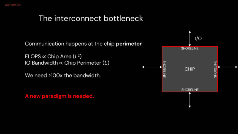
One of the observations is that compute is scaling faster than interconnect.

One of the big challenges is that the chip perimeter has the shoreline used for off-chip I/O. That physical area restriction limits how much I/O can happen.
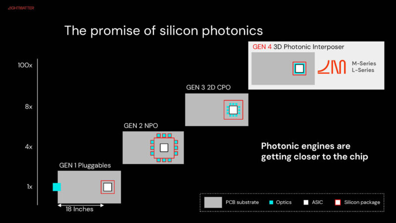
Lightmatter is talking about the benefits of moving silicon photonics closer to the chip. The Gen 1 would be something like the Intel Silicon Photonics 100GbE QSFP28 500m Optic.
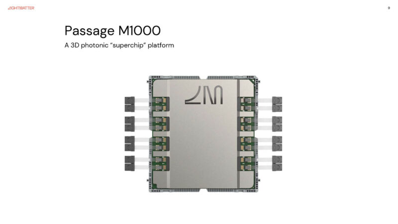
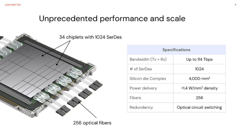
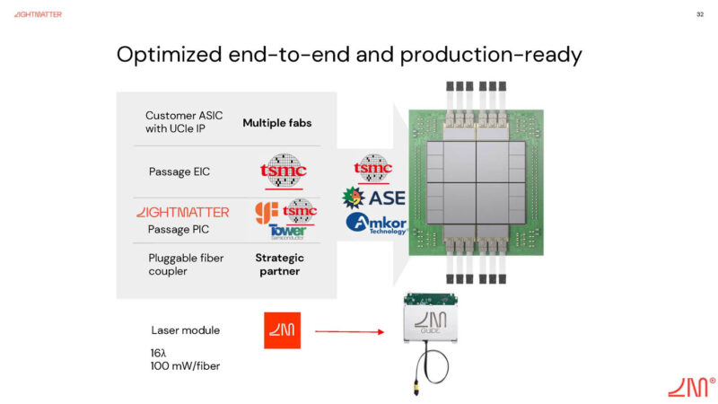
Lightmatter’s new solution is the Passage M1000.
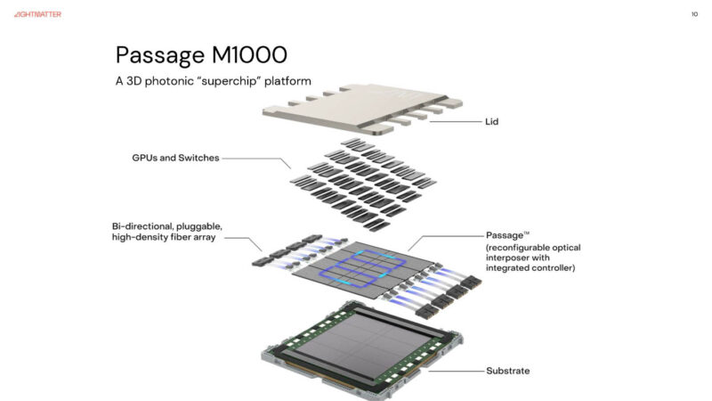
The idea is that there can be compute and memory chiplets packaged atop the Passage optical interposer.
The new design promises up to 114Tbps which seems to be 57Tbps in each direction.
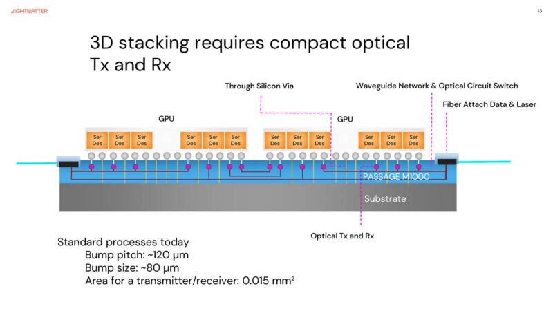
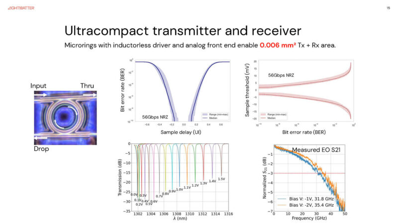
With 3D stacking chips the optical transmitter/ receiver needs to be compact. The GPU chiplets connect to the SerDes that are connected to the optical side on the Passage M1000. The challenge is that that you want the optical components to match the physical size of the electrical SerDes so that you can maintain density across the package.
Lightmatter is using silcon microrings to modulate the light.
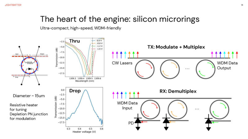
These microrings enable very compact optical I/O.
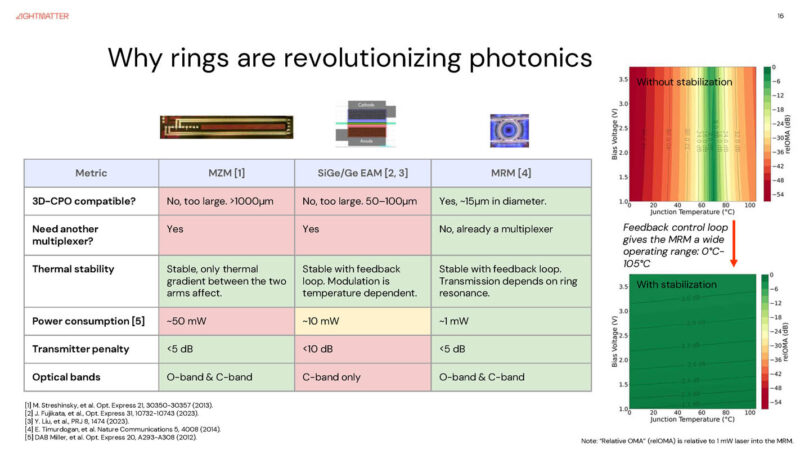
This is fun. Lightmatter is showing why microrings are the best. Celestial AI just had a similar chart two talks ago showing why it is using EAM.
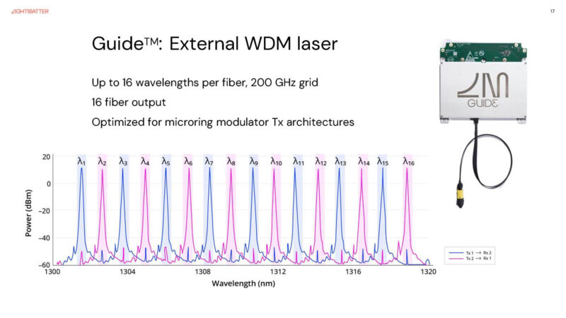
Lightmatter has its own 16 wavelength laster called the Lightmatter Guide
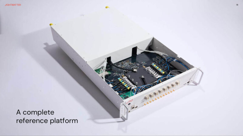
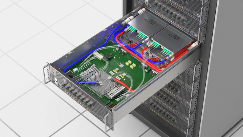
Lightmatter has a reference platform.
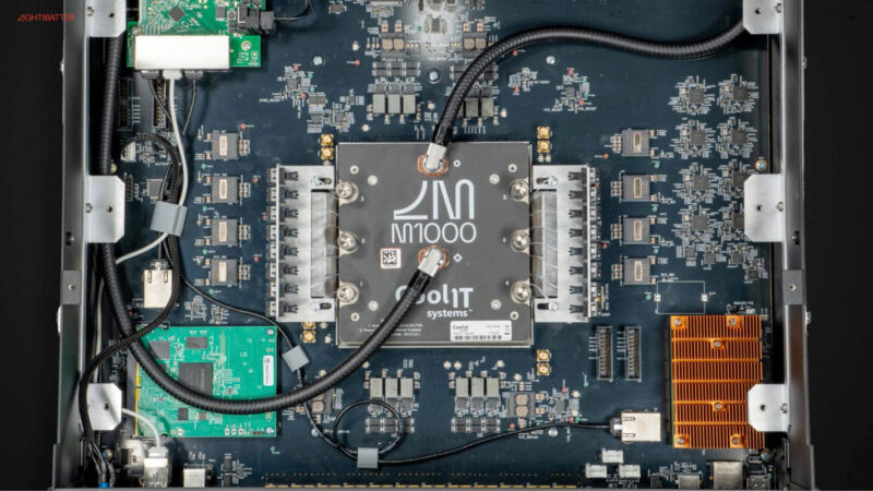
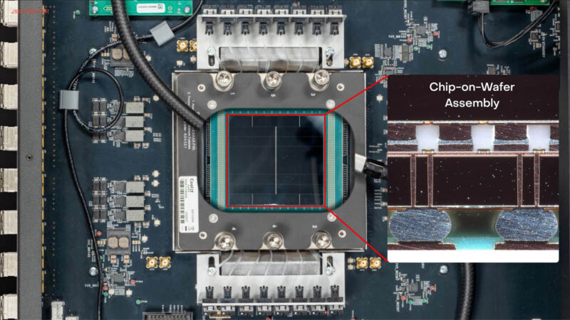
Here is a look at the Passage M1000 with a CoolIT liquid cooler on top.
Here is what this looks like with the chip-on-wafer assembly.
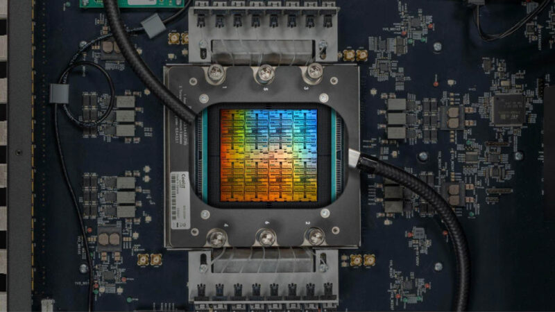
Here is a colorized version.
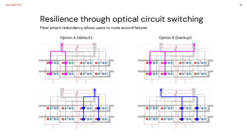
Passage M1000 also has some reconfigurability.
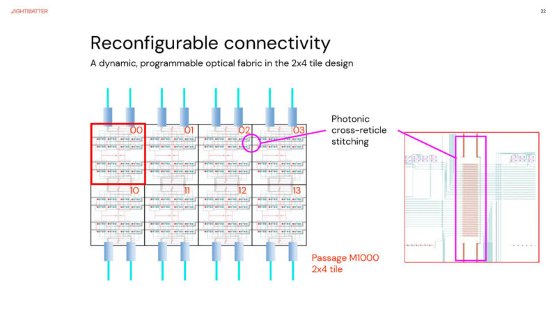
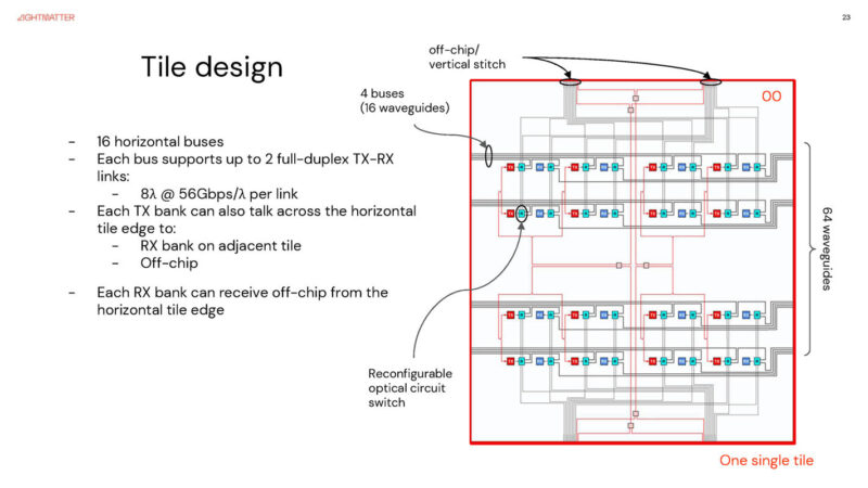
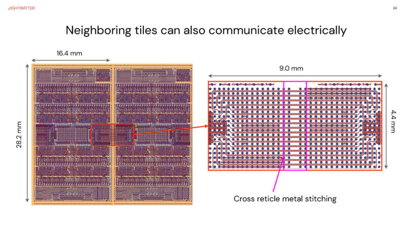
Here is a bit more on the tile design with the 16 horizontal busses and how they connect to the off-chip links.
Here is the cross retical metal stitching for electrical connectivity.
Lightmatter says that it has optical circuit switching for redundancy.
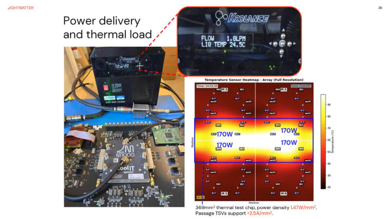
Here is a test rig with the power and thermal load being applied.
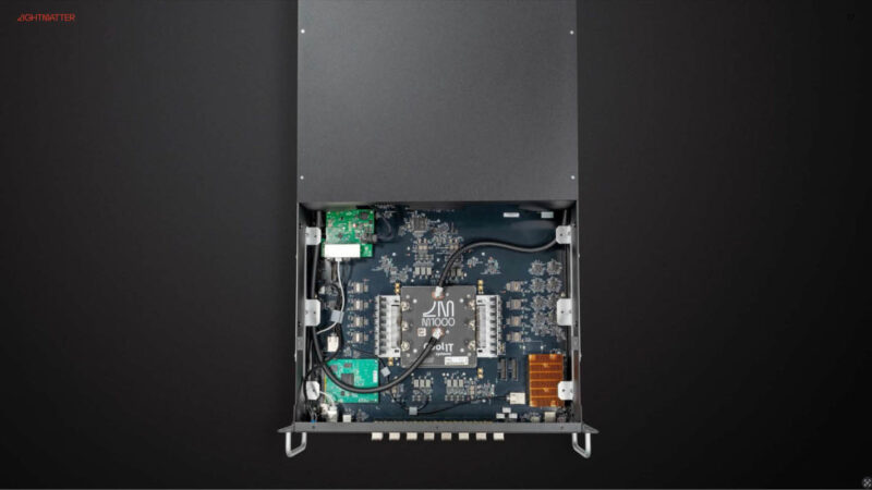
Here is a top view of the appliance.
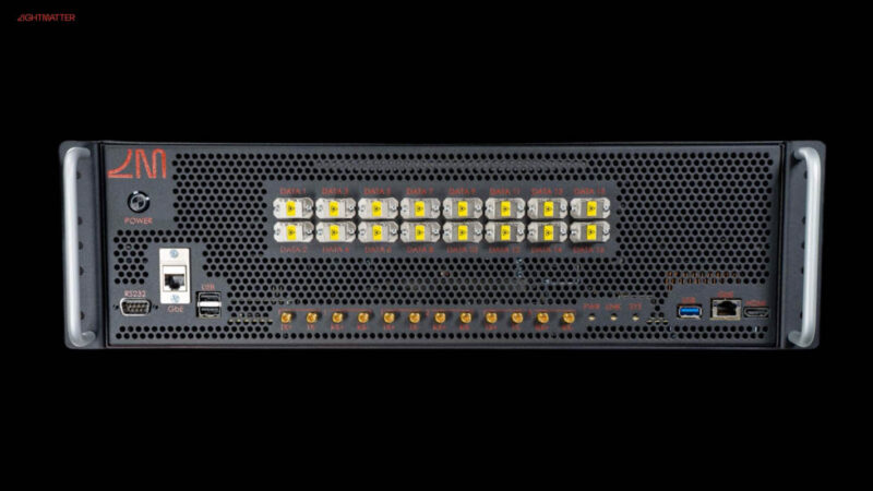
Here is the 16 optical connectors on the front of the reference appliance.
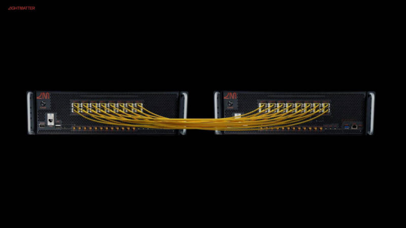
Here is what two look like connected together.
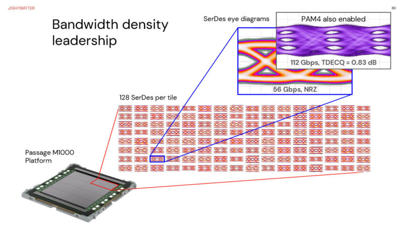
There is a ton of bandwidth enabled on the interposer platform.
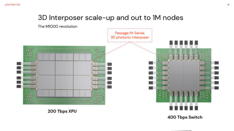
M1000 is the first step towards construction of having XPUs with more than 200Tbps and switches with more than 400Tbps of bandwidth. Just for reference, a high-end Broadcom Tomahawk 6 is a 102.4T switch chip.
Lightmatter says it is production ready.
Here is another look at what this could look like.
Final Words
I have always thought Lightmatter has a really neat platform. For me, the big question is not whether this is a great idea. My bigger question is when will this finally run in the wild. The company said it will be on public demo at SC25 this year.


Yeah, this is cool. Seeing the similarities between this and the ones from Ayar Labs and Celestial AI makes me think that the various companies doing this sort of thing are pretty much converging on a single standard way of implementing photonic circuits. It would be neat if they could devise some way of making this technology actually capable of performing computation and not just acting as super-speed interconnects.