
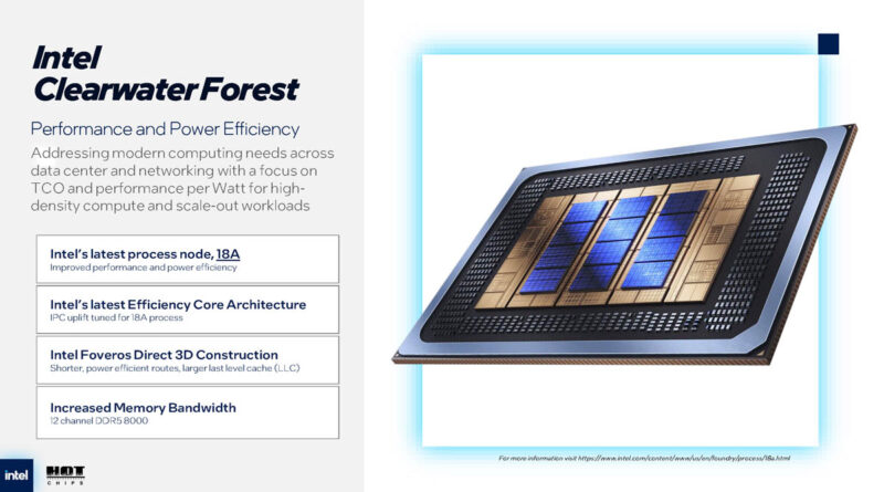
At Hot Chips 2025, Intel went into its next-gen 288-core processor. Constructed on Intel 18A process and using 3D packaging technology, this is a major leap over the previous generation Sierra Forest with more cache, faster E-cores, and more memory bandwidth.
Please note, we are covering this live, so please excuse typos.
Intel Xeon Clearwater Forest with 288 Cores on Intel 18A at Hot Chips 2025
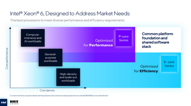
The second of Intel’s Forest chips, Clearwater Forest follows Sierra as Intel’s many-core focused design. Rather than relying on Intel’s traditional big cores (P-cores), the Forest chips are comprised entirely of the smaller efficiency cores. This makes them aimed at workloads that need to run many different threads in a power efficient manner – but not necessarily requiring the highest possible performance per thread.
Clearwater Forest has been in Intel’s labs for several months now, and will be moving to production very soon. It’s one of their first Intel 18A process chips, so it’s important for the company on multiple levels.
Clearwater Forest will use the same platform as Intel’s current Xeon 6 generation chips (Granite Rapids & Sierra Forest).
Power efficiency is the name of the game for Clearwater. And it’s something Intel is promising (threatening?) to repeat ad infinitum during this talk. 18A brings a big jump in power efficiency, but also core architecture improvements as well.
Another big part is the switch to using 3D die stacking, accomplished via Foveros Direct 3D.
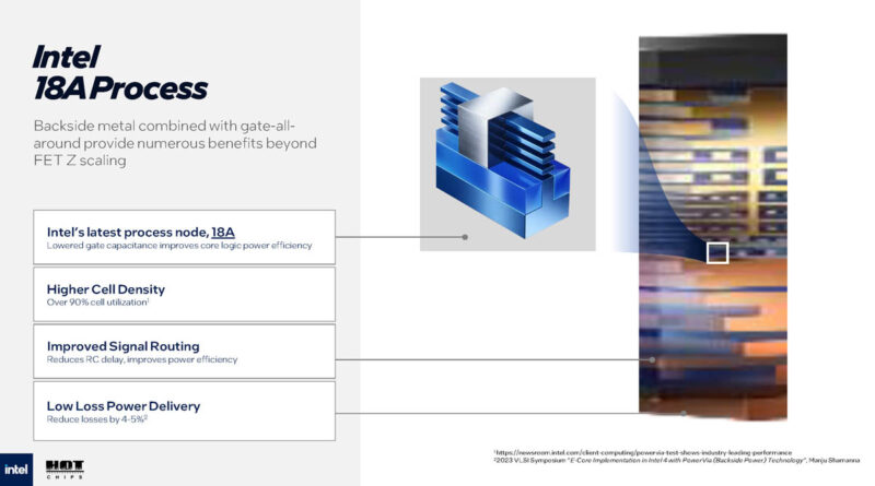
The 18A process brings several innovations. Intel is particularly focused on backside metal/backside power delivery, delivering power (and putting the rails for that) from behind the transistors instead of on top of them. (This is also a big point for Intel because it’s a technology they’re well ahead of TSMC on)
BSPDN also delivers some cell density improvements, with Intel reporting that they’ve hit over 90% cell utilization.
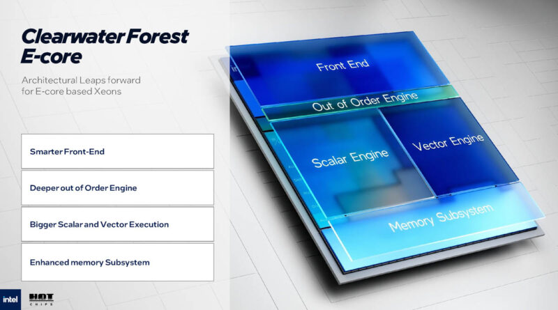
As for the architecture itself, Intel says that the architecture impact to Clearwater’s energy efficiency improvements should not be underestimated. There are 4 contributing factors here:
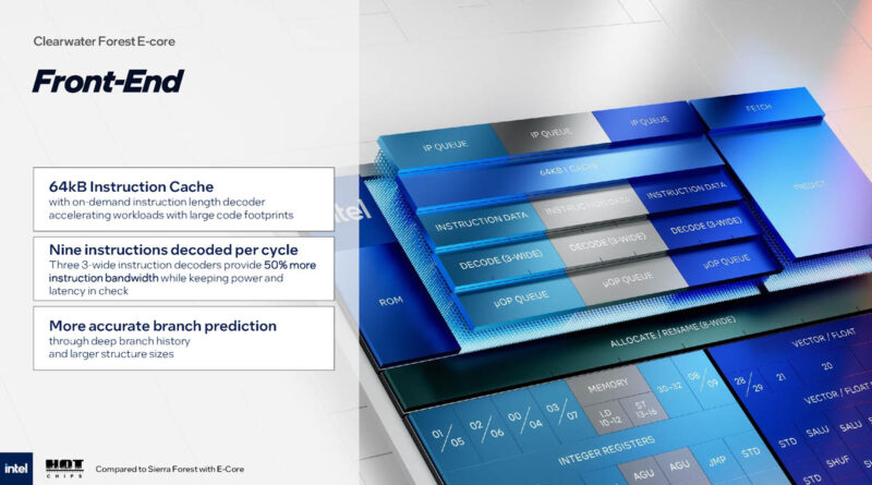
Compared to Sierra Forest, Clearwater goes from 6-wide deocde to 9-wide decode, via a trio of 3-wide decoders. The branch predictor has also been improved, both to keep pace with the wider front-end and to improve accuracy overall.
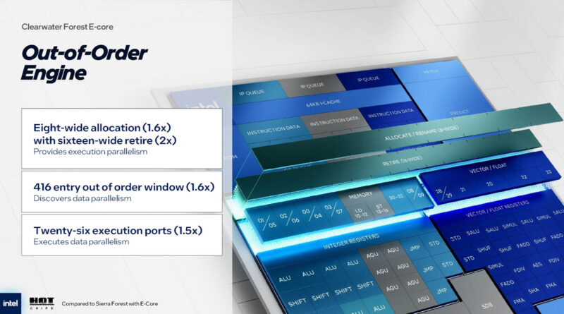
On the back-end of things, the out-of-order execution engine has gone from being able to dispatch 5 ops to clock to 8 ops. Altogether, 16 ops can be retired per clock, which is 2x Sierra.
And the number of execution ports has been greatly increased as well, bringing Clearwater to 26 execution ports – despite being a small efficiency core!
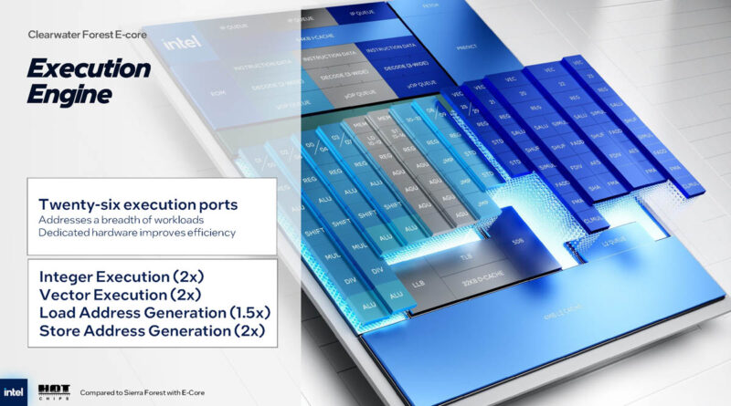
Integer and vector execution throughput has been doubled. So has store address generation. Only load address generations have not been doubled – those are “just” 1.5x Sierra.
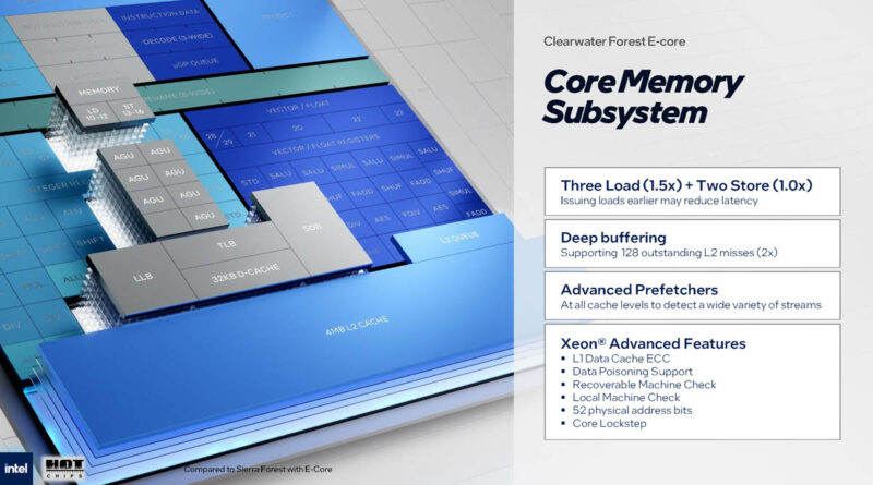
As for the memory interface, the L2 miss buffer has been doubled in size, bringing it to store 128 misses. This is directly coupled to Clearwater’s overall memory bandwidth, and Intel had to expand it in proportion to the additional bandwidth Clearwater will offer.
And while it’s a bit of a footnote, there’s several RAS features here enabled by the core.
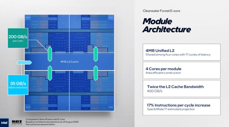
Going up a level, a single Clearwater Forest module is 4 cores, sharing a 4MB united L2, just like it was on Sierra. Though L2 cache bandwidth has been doubled to 400GB/sec.
As for performance Intel is claiming a 17% IPC uplift on SPECint 2017.
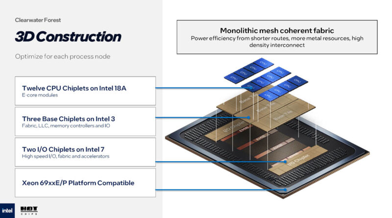
Unlike Sierra, which was a 2.5D design, Clearwater Forest is a 3D design, with CPU chiplets on top of larger base dies with the rest of the uncore hardware.
Doing a bit of math on the specs, the 1152MB of LLC means we have 576MB of last level cache per socket. That was only 108MB per 144 core tile or 216MB total on Sierra Forrest 288 core. We also have 576 cores in the platform or 288 per socket.
The base die is built on the Intel 3 process. And the IO Die is reused from Sierra Forest, where it was built on the Intel 7 process.
Intel is still using EMIB for die-to-die interconnects as well.
12 CPU chiplets, 3 base dies, 2 I/O dies.
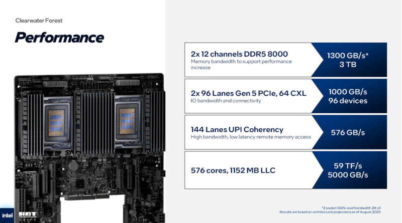
In a two socket system, each chip has 12 channels of DDR5-8000 memory (standard, not MRDIMM). For a total of 1300GB/sec of memory bandwidth (apparently 100% read; actualized capabilities).
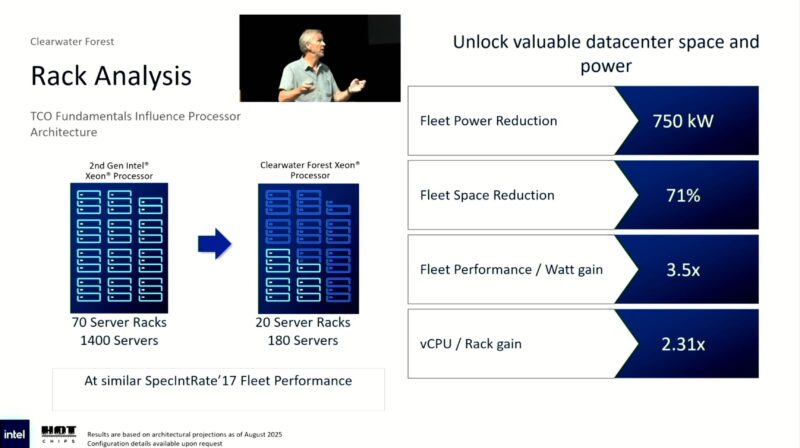
Also a quick look at things in terms of racks. With datacenters being constrained on power, being able to consolidate in order to reduce power consumption – and thus TCO – can be a very big deal. Altogether, versus Sierra, Intel is claiming that Clearwater racks will be able to offer 3.5x perf-per-watt gain.


This is really cool. Just curious if this is the generation where the e-cores get avx10.2 (avx-512) support? Its been really confusing to follow when its coming and I was curious if having the avx-512 support could impact the performance/power ratio especially since certain work loads benefit more and if there would be a heat concern if all 288 cores run avx-512 instructions(I know its probably not likely just curious). Also since the memory controller is on the base chiplet unlike in sierra forest where I believe it was on the same die as the core is there any concerns of memory latency issues? Also is it known if the memory controller is the same as from sierra since both are made on intel 3? If so would that be a good sign for the foundries use of industry standard EDA, and potentially make optimization easier for memory based work loads??
I believe avx10.2 will first arrive in Diamond Rapids.
They do say they’ve doubled some SIMD relative to Sierra Forest, but I’m guessing that means doubling to two AVX2 FMA units…
@JayN
This core is based off Skymont on Arrowlake and Lunarlake, the Core 200 series chips.
Skymont has 4x 128-bit FMA, versus 2x 128-bit FMA for Crestmont.
I think it is more accurate to say that in today’s hotchips 2025 presentation, Intel did not disclose the design of the FMA units of the Darkmont cores that are used in Clearwater Forest.
So this is an AP vs SP based on the 12ch memory?
Something brought up on Chips and Cheese is that Intel skymont can be produced on both Intel 18A and TSMC 3nm.
Would be interesting once everything is available to do a head to head between manufacturing processes using the same core architecture.